Getting Started with the EVBMA6X02BMU Evaluation Board
Contents of this document
-
Out of the Box
-
Get to Know the Hardware
-
Configure Hardware
-
Install Software
Sign in to save your progress. Don't have an account? Create one.
Purchase your Optimized Battery Management Unit with BMA6X02
1. Out of the Box
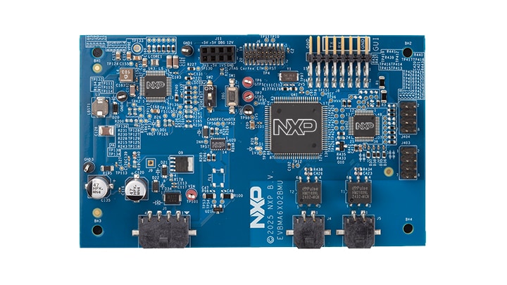
The EVBMA6X02BMU is an evaluation board composed of all necessary headers, jumpers and signal test points to quickly evaluate NXP products.
This document is intended to help a user quickly set up, configure, and operate the EVBMA6X02BMU evaluation board.
1.1 Kit Contents and Packing List
The kit contents include:
- EVBMA6X02BMU - optimized battery management unit
- Power supply (12 V)
- Cable for supply and CAN interface
- ETPL cable - two-wire twisted pair TPL cable (50 cm)
- 3.3 V FTDI cable
1.2 Additional Hardware
In addition to the kit contents, the following hardware is necessary or beneficial when working with this board.
- Power cord to connect the power supply to the grid
- Additional AFE boards (for example, EVBMA7118 or EVBMA777T2) that should be controlled by the EVBMA6X02BMU board
- PC with programming environment for the S32K358 and associated debug probes
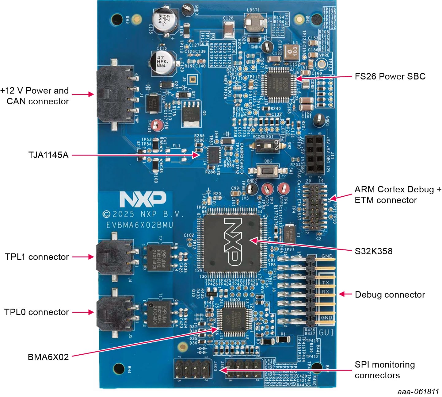
2. Get to Know the Hardware
2.1 Board Features
- MCU (S32K358)
- SBC (FS26)
- Communication gateway (BMA6X02S)
2.2 Board Description
The key components are listed in Table 1.
| Component | Description |
|---|---|
| U43 - FS2633D | SBC to generate the supplies for all components on the board |
| U31 - S32K358 | MCU to control the board |
| U402 - BMA6X02S | GTW to allow communication to the other boards of the battery management systems |
| U20 - TJA1145A | CAN transceiver to allow communication to other CAN devices |
3. Configure Hardware
The EVBMA6X02BMU has several configuration options. The most important ones are the clock and SPI configuration of the BMA6X02S.
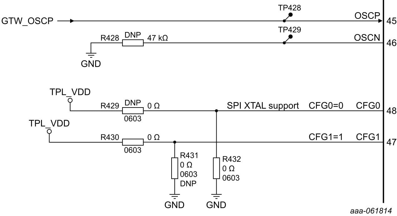
3.1 Clock Configuration
The BMA6X02S has three clock configuration options. It can operate with an internal clock, an external crystal or an external clock source. The default configuration is the external clock source, where it is assumed that the S35K358 is configured to provide this clock to the pin OSCP. The OSCP pin is connected on the board
to the pin PTB5_47_CLKOUT_RUN_TP8. A change of the clock source selection can be done with R429, R430, R431 and R432 (see Figure 2). Refer to the BMA6X02S data sheet for details on how to change the configuration.
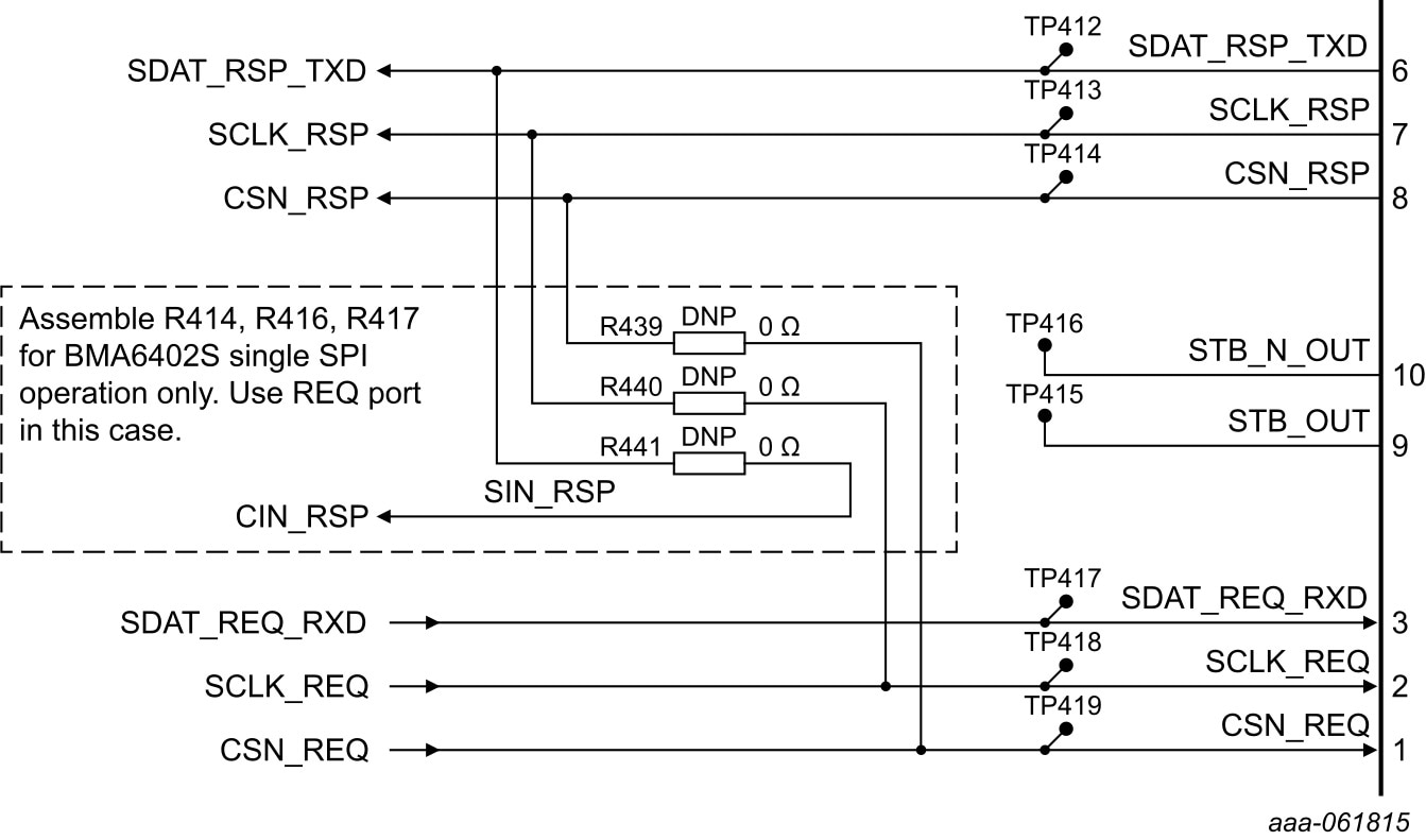
3.2 SPI Configuration
The BMA6X02S has three SPI configurations. It can operate as a single or a dual SPI with the response SPI as a controller or a target. The default configuration of the EVBMA6X02BMU is the dual SPI configuration. The configuration can be changed with R439, R440 and R441 (see Figure 3). Ensure that the hardware configuration used is matching to the software configuration of the S32K358.
4. Install Software
4.1 Install Software
Download and install the following software:
Note: There are some requisites to obtain the software.
- An NDA agreement with NXP
Design Resources
Board Information
Additional References
In addition to the BMX6X02, General-Purpose Battery Management System Communication Gateway, visit:
Automotive
Industrial