Design Files
1 design file
Receive the full breakdown. See the product footprint and more in the eCad file.
-
Models
CBTU02044 S-Parameter Model
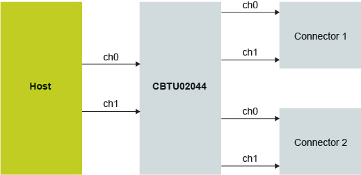
CBTU02044 is a high-speed differential 1-to-2 switching chip optimized to interface with PCIe4.0 for server and client applications. This high performance switch chip could be used for other high-speed interfaces such as PCIe-Gen4, MIPI, DP1.4 and DDR.
CBTU02044 also functions as a 2-to-1 MUX by selecting 1 (Port A) as output out of one of the two differential ports (either Port B or C). Pinouts are optimized for minimum number of layout layers and for achievement of very low crosstalk to meet stringent crosstalk requirements at higher data rate.
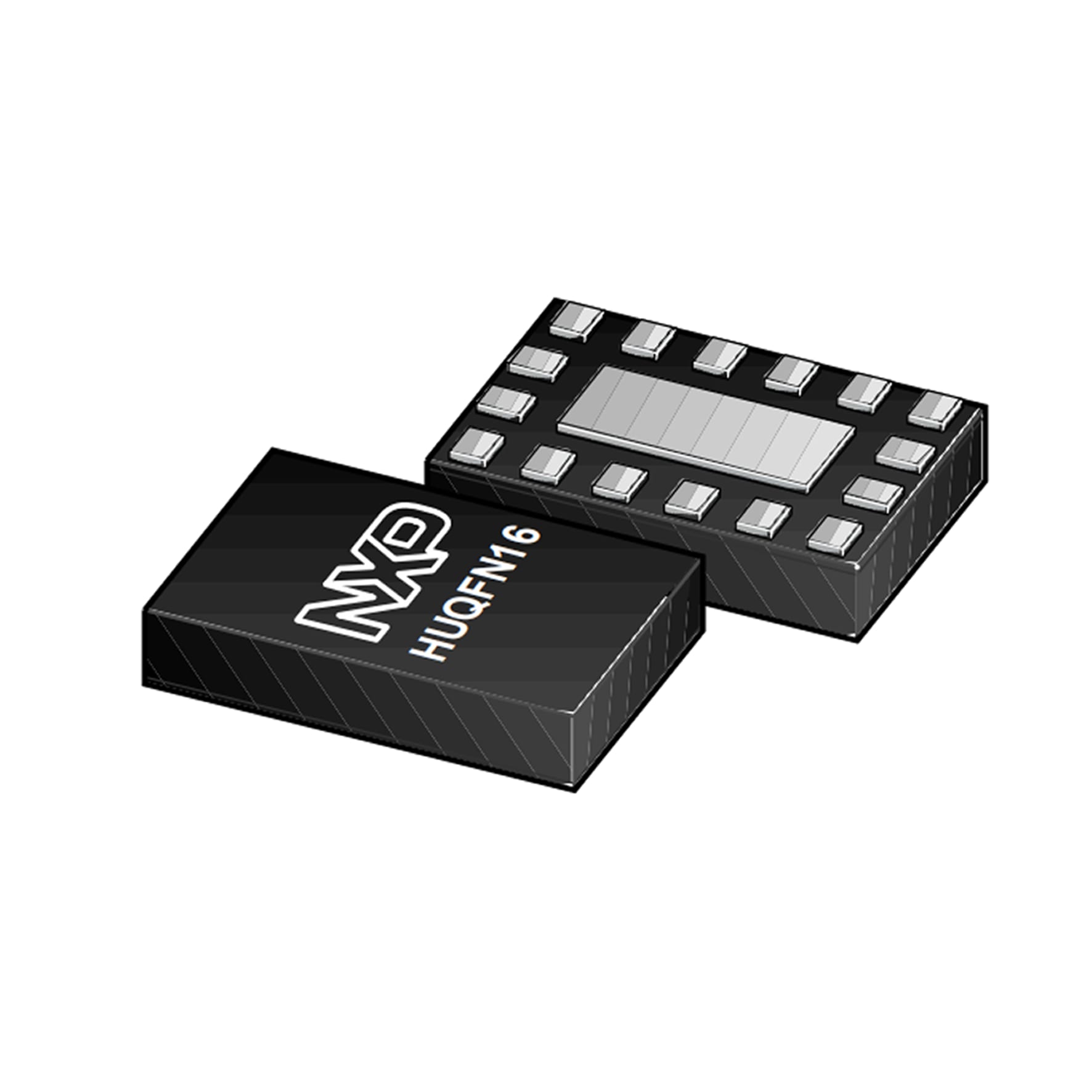
CBTU02044 is a small package with optimized footprint for smaller real estate occupancy and is available in 1.6 mm x 2.4 mm x 0.5 mm HUQFN16 package with 0.4 mm pitch.

Choose a diagram:

Note: To see the product features close this window.
|
|
|
|
|
|
|
|---|---|---|---|---|---|
|
|
|
|
|
|
|
|
|
|
|
|
|
|
|
|
|
|
|
|
|
|
|
|
|
|
|
|
|
|
|
|
|
|
|
|
|
|
|
|
|
|
|
|
|
|
|
|
|
|
|
|
|
|
|
|
|
|
|
|
|
|
|
|
|
|
|
|
|
|
Quick reference to our documentation types
3 documents
Compact List
Please wait while your secure files are loading.
1 design file
Receive the full breakdown. See the product footprint and more in the eCad file.
Please wait while your secure files are loading.