
Application Note (2)
Brochure (2)
Data Sheet (1)
Package Information (2)
Packing Information (2)
User Guide (3)
-
UM10323[UM10323]
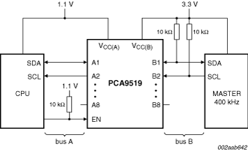
The PCA9519 is a 4-channel level translating I²C-bus/SMBus repeater that enables the processor low voltage 2-wire serial bus to interface with standard I²C-bus or SMBus I/O. While retaining all the operating modes and features of the I²C-bus system during the level shifts, it also permits extension of the I²C-bus by providing bidirectional buffering for both the data (SDA) and the clock (SCL) lines, thus enabling the I²C-bus or SMBus maximum capacitance of 400 pF on the higher voltage side. The SDA and SCL pins are over-voltage tolerant and are high-impedance when the PCA9519 is unpowered.
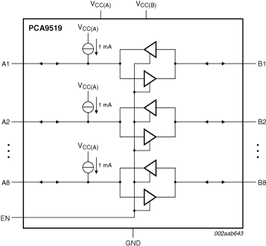
The port B drivers are compliant with SMBus I/O levels, while port A uses a current sensing mechanism to detect the input or output LOW signal which prevents bus lock-up. The port A uses a 1 mA current source for pull-up and a 200 Ω pull-down driver. This results in a LOW on port A accommodating smaller voltage swings. The output pull-down on the port A internal buffer LOW is set for approximately 0.2 V, while the input threshold of the internal buffer is set about 50 mV lower than that of the output voltage LOW. When the port A I/O is driven LOW internally, the LOW is not recognized as a LOW by the input. This prevents a lock-up condition from occurring. The output pull-down on the port B drives a hard LOW and the input level is set at 0.3 of SMBus or I²C-bus voltage level which enables port B to connect to any other I²C-bus device or buffer.
The PCA9519 drivers are not enabled unless VCC(A) is above 0.8 V and VCC(B) is above 2.5 V. The enable (EN) pin can also be used to turn the drivers on and off under system control. Caution should be observed to only change the state of the EN pin when the bus is idle.
Choose a diagram:
|
|
|
|
|
|
|
|---|---|---|---|---|---|
|
|
|
|
|
|
|
|
|
|
|
|
|
|
|
|
|
|
|
|
|
|
|
|
|
|
|
|
|
|
|
|
|
|
|
|
|
|
|
|
|
|
|
|
|
|
|
|
|
|
|
|
|
|
|
|
|
|
|
|
|
|
|
|
|
|
|
|
|
|
Quick reference to our documentation types
1-10 of 12 documents
Compact List
2 design files
Receive the full breakdown. See the product footprint and more in the eCad file.
To get further assistance directly from NXP, please see our Engineering Services.
2 engineering services

To find additional partner offerings that support this product, visit our Partner Marketplace.