Product Longevity
Participating products are available for a minimum of 10 years. Designated participating products developed for the automotive, telecom and medical segments are available for a minimum of 15 years.
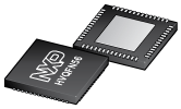
PTN3460 is an (embedded) DisplayPort to LVDS bridge device that enables connectivity between an (embedded) DisplayPort (eDP) source and LVDS display panel. It processes the incoming DisplayPort (DP) stream, performs DP to LVDS protocol conversion and transmits processed stream in LVDS format.
PTN3460 has two high-speed ports: Receive port facing DP Source (for example, CPU/GPU/chip set), Transmit port facing the LVDS receiver (for example, LVDS display panel controller). The PTN3460 can receive DP stream at link rate 1.62 Gbit/s or 2.7 Gbit/s and it can support 1-lane or 2-lane DP operation. It interacts with DP source via DP Auxiliary (AUX) channel transactions for DP link training and setup.
It supports single bus or dual bus LVDS signaling with color depths of 18 bits per pixel or 24 bits per pixel and pixel clock frequency up to 112 MHz. The LVDS data packing can be done either in VESA or JEIDA format. Also, the DP AUX interface transports I²C-over-AUX commands and support EDID-DDC communication with LVDS panel. To support panels without EDID ROM, the PTN3460 can emulate EDID ROM behavior avoiding specific changes in system video BIOS.
PTN3460 provides high flexibility to optimally fit under different platform environments. It supports three configuration options: multi-level configuration pins, DP AUX interface, and I²C-bus interface.
PTN3460 can be powered by either 3.3 V supply only or dual supplies (3.3 V / 1.8 V) and is available in the HVQFN56 7 mm x 7 mm package with 0.4 mm pitch.
Participating products are available for a minimum of 10 years. Designated participating products developed for the automotive, telecom and medical segments are available for a minimum of 15 years.
|
|
|
|
|
|
|
|---|---|---|---|---|---|
|
|
|
|
|
|
|
|
|
|
|
|
|
|
|
|
|
|
|
|
|
|
|
|
|
|
|
|
|
|
|
|
|
|
|
|
|
|
|
|
|
|
|
|
|
|
|
|
|
|
|
|
|
|
|
|
|
|
|
|
|
|
|
|
|
|
|
|
|
|
Quick reference to our documentation types
7 documents
Compact List
Receive the full breakdown. See the product footprint and more in the eCad file.
1 hardware offering
To get further assistance directly from NXP, please see our Engineering Services.
2 engineering services

To find additional partner offerings that support this product, visit our Partner Marketplace.
