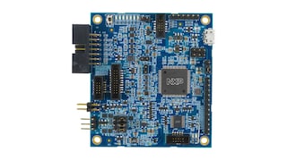
The LPC546xx MCU family combines the power efficiency of the 220 MHz Arm® Cortex®-M4 core with multiple high-speed connectivity options, advanced timers, and analog features. DSP capabilities enable LPC546xx MCU devices to support complex algorithms in data-intensive application. Providing flexibility with up to 512 KB Flash and external memory interfaces, this family provides the ability to adapt as requirements change. Flash options support large, flexible internal and external memory configurations. Compatibility within the LPC54000 series enables the LPC546xx MCU family to provide a seamless migration path for increasing processing power and adding the flexibility of additionally advanced peripherals.
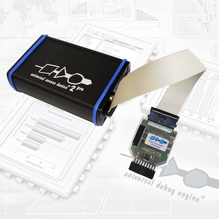
This device is fully supported by NXP’s MCUXpresso Software and Tools, a comprehensive and cohesive set of free software development tools for Kinetis, LPC and i.MX RT microcontrollers. MCUXpresso SDK also includes project files for Keil MDK and IAR EWARM.