Getting Started with the KITPF51SKTEVM Evaluation Board
Contents of this document
-
Out of the Box
-
Get to Know the Hardware
-
Configure the Hardware
Sign in to save your progress. Don't have an account? Create one.
Purchase your KITPF51SKTEVM
1. Out of the box
The NXP analog product development boards provide an easy-to-use platform for evaluating NXP products. The boards support a range of analog, mixed-signal and power solutions. They incorporate monolithic integrated circuits and system-in-package devices that use proven high-volume technology. NXP products offer longer battery life, a smaller form factor, reduced component counts, lower cost, and improved performance in powering state-of-the-art systems.
This page will guide you through the process of setting up and using the KITPF51SKTEVM board.
1.1 Kit Contents and Packing List
Working with the KITPF51SKTEVM requires the kit contents, more hardware, and a Windows PC workstation with installed software.
The kit contents include:
- Assembled and tested evaluation board in an antistatic bag
- Quick start guide
- An assembled and tested evaluation board and preprogrammed FRDM-KL25Z microcontroller board in an anti-static bag
- A 3.0 ft USB-STD A to USB-C-minicable
- Jumpers mounted onboard
1.2 Additional hardware
In addition to the kit contents, the following hardware is necessary or beneficial when working with this board:
- A power supply with a range of 3.3 V to 5.0 V
1.3 Minimum System Requirements
This evaluation board requires a Windows PC workstation. Meeting these minimum specifications should produce great results when working with this evaluation board:
- USB-enabled computer with Windows 7 or Windows 10
1.4 Software
Installing software is necessary to work with this evaluation board. All listed software is available on the NXP GUI for Automotive PMIC Families information page at PMIC-GUI-SW.
2. Get to Know the Hardware
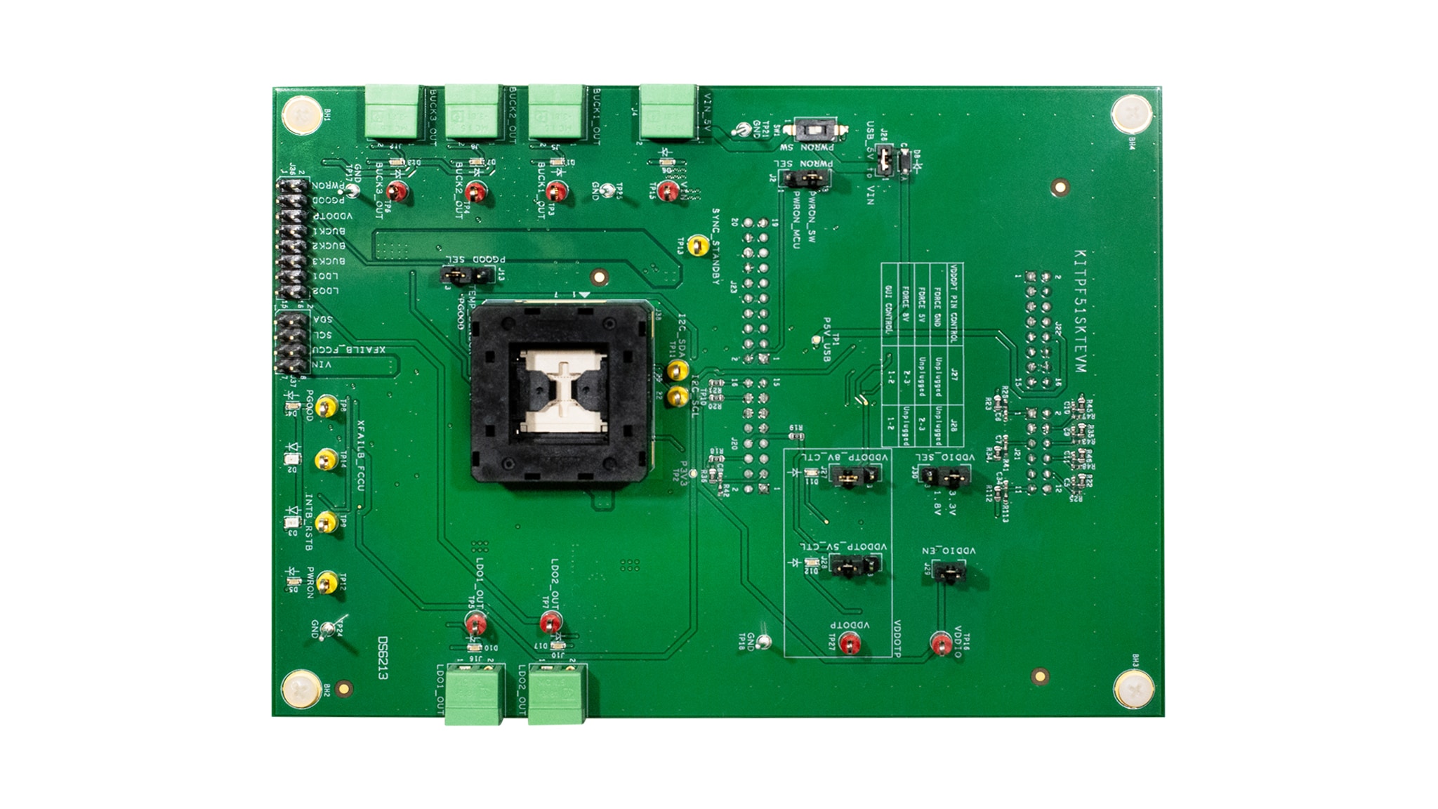
The KITPF51SKTEVM kit provides an integrated platform for evaluating designs based on NXP's PF5103, PF5113, PF5123, and PF0300 PMICs. All PF51 family features can be accessed and monitored in a test environment.
The kit hardware consists of the KITPF51SKTEVM evaluation board, a FRDM-KL25Z microcontroller board, and the USB cable required to connect the FRDM-KL25Z to the PC.
The KITPF51SKTEVM evaluation board features a socket that allows users to flash an individual PF5103, PF5113, PF5123, or PF0300 using the device's one time programmable (OTP) feature. Connectors, jumpers, and switches on the board can be used to configure an evaluation environment that meets specific design requirements. The board also contains LEDs and test points that provide a means of monitoring performance in real time.
The FRDM-KL25Z is mounted to Arduino connectors on the bottom of the KITPF51SKTEVM board.The role of the FRDM-KL25Z is to manage SPI communication between the KITPF51SKTEVM board and the GUI installed on the PC. The FRDM- KL25Z draws power from the USB cable connected to the PC.
This document uses the PF5103 as a default configuration. Specificities for PF5113, PF5123, or PF0300 are explained in the flow if necessary. Otherwise, the features are common to PF51xx.
2.1 Board Features
- Phoenix (3.81mm) male connectors for switches and LDOs
- Selectable Debug mode, Normal mode, and Test mode
- VDDOTP and PWRON to power up the device in different modes
- PGOOD, INTB/RSTB, SYNC and XFAIL pins
- USB to I²C protocol for easy connection to software GUI
- LEDs, green and red, indicate signal or regulator status
- LED blue to indicate VDDOTP pin is set to 8 V (OTP burning voltage)
- Header connectors for monitoring outputs
- Advanced system monitoring via KL25 MCU ADC
2.2 Board Components
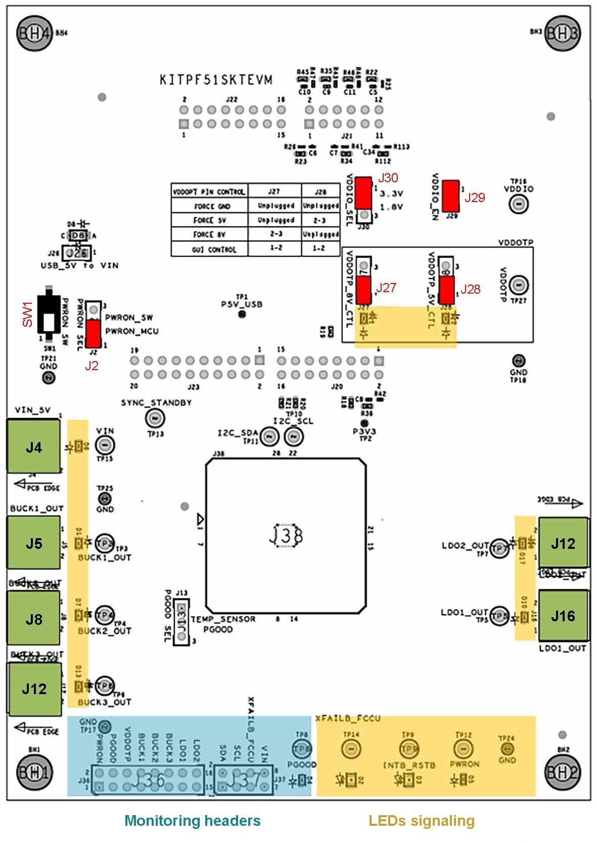
| Position | Function | Description |
|---|---|---|
J2 |
PWRON_SEL | PWRON controlled either by MCU or manually with PWRON_SW |
J4 |
VIN | Input voltage (3.3 V min/5.5 V max) |
J5 |
BUCK1_OUT | Output for Buck 1 |
J8 |
BUCK2_OUT | Output for Buck 2 |
J10 |
LDO2_OUT | Output for LDO 2 |
J12 |
BUCK3_OUT | Output for Buck 3 |
J13 |
PGOOD_SEL | PGOOD setting either PGOOD/GPO or output of temperature junction analog voltage |
J16 |
LDO1_OUT | Output for LDO 1 |
J26 |
USB_5V_TO_VIN | Supply VIN with 5 V from USB (Current limited to 1A) |
J27 |
VDDOTP_8V_CTL | 8 V on VDDOTP controlled either manually or by MCU |
J28 |
VDDOTP_5V_CTL | 5 V on VDDOTP controlled either manually or by MCU |
J29 |
VDDIO_EN | Apply VDDIO to VDDIO pin |
J30 |
VDDIO_SEL | VDDIO set to either 1.8 V or 3.3 V |
J36/J37 |
Monitoring headers | I/O pins and regulators outputs for monitoring purpose |
| SW1 | PWRON_SW | PWRON manual control (assume J2 on PWRON_SW position) |
3. Configure the Hardware
3.1 Configure the Hardware
The procedure for setting up the KITPF51SKTEVM board is as follows:
- Make sure the board has the jumpers and switch configured in their default positions. The default
configuration enables the board to be fully controlled by the FRDM-KL25Z and the GUI. Figure 2 shows the
default jumper and switch configuration for a PF5103 part only.
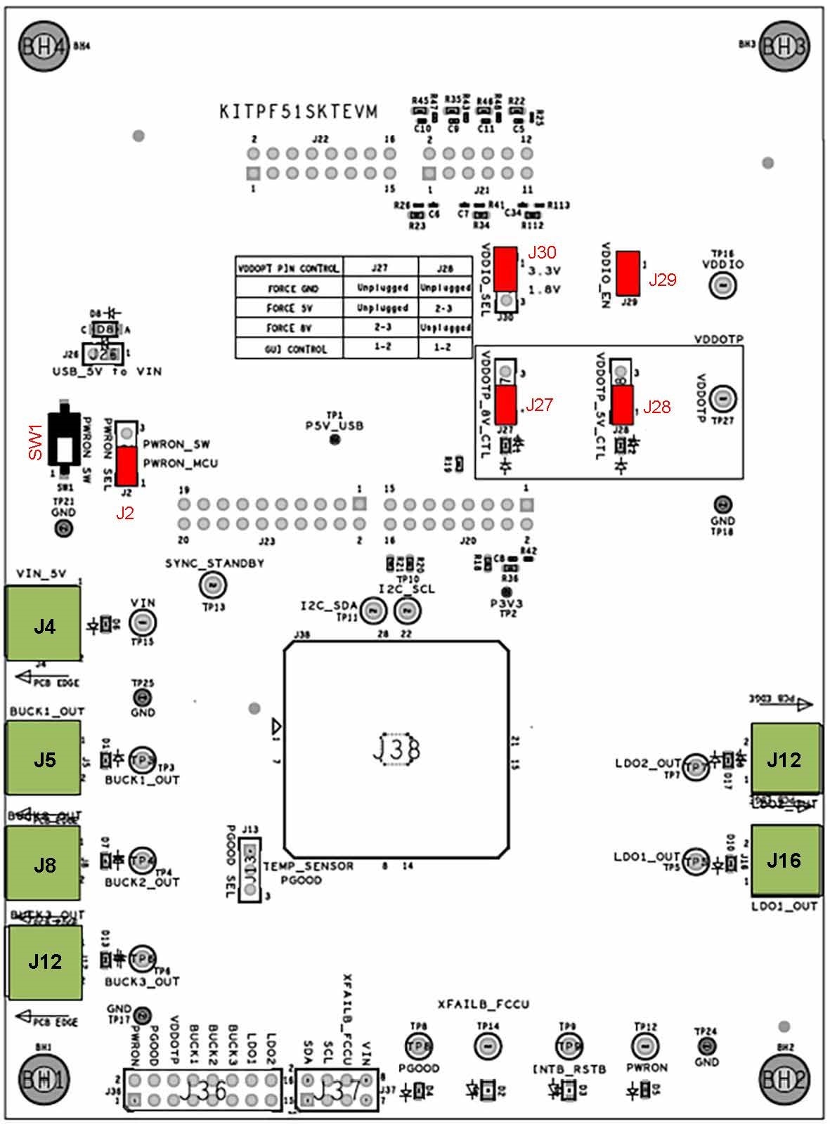
- Connect the power supply to
J4(Phoenix connector - 3.81 mm). The power supply should be set to an initial value of 5.0 V. - Verify the FRDM-KL25Z board is firmly mounted to the KITPF51SKTEVM board. Ensure the USB cable between the FRDM-KL25Z and the PC is securely connected. The USB port serves as a communication channel between the PC and the FRDM-KL25Z board and provides voltages and references to some onboard circuits. It also generates the VDDIO reference for the IC.
Design Resources
Board Information
Additional References
In addition to our PF51x3: Production description page, you may also want to visit:
Product pages: