
Product Longevity
Participating products are available for a minimum of 10 years. Designated participating products developed for the automotive, telecom and medical segments are available for a minimum of 15 years.
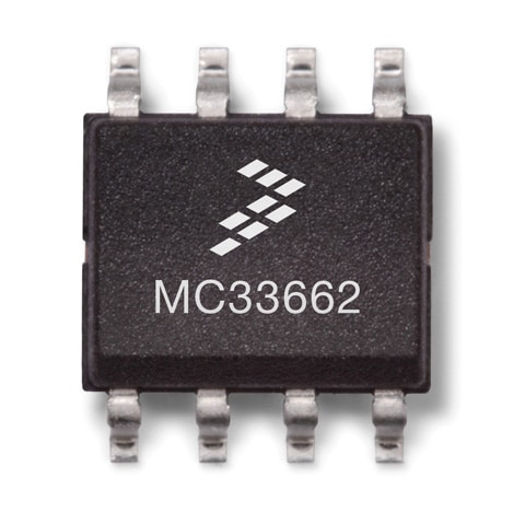
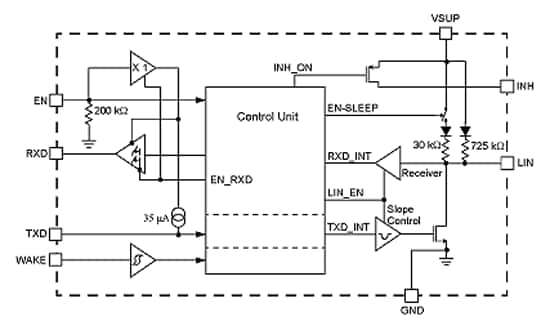
The NXP MC33662 is a physical layer component dedicated to automotive LIN sub-bus applications.
Note: To see the product features close this window.

Participating products are available for a minimum of 10 years. Designated participating products developed for the automotive, telecom and medical segments are available for a minimum of 15 years.
|
|
|
|
|
|
|
|---|---|---|---|---|---|
|
|
|
|
|
|
|
|
|
|
|
|
|
|
|
|
|
|
|
|
|
|
|
|
|
|
|
|
|
|
|
|
|
|
|
|
|
|
|
|
|
|
|
|
|
|
|
|
|
|
|
|
|
|
|
|
|
|
|
|
|
|
|
|
|
|
|
|
|
|
Quick reference to our documentation types
4 documents
Compact List
Please wait while your secure files are loading.
Receive the full breakdown. See the product footprint and more in the eCad file.

Receive the full breakdown. See the product footprint and more in the eCad file.
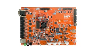
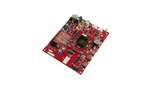
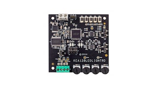
1-5 of 6 hardware offerings

2 engineering services


There are no results for this selection.
To find additional partner offerings that support this product, visit our Partner Marketplace.
1 trainings