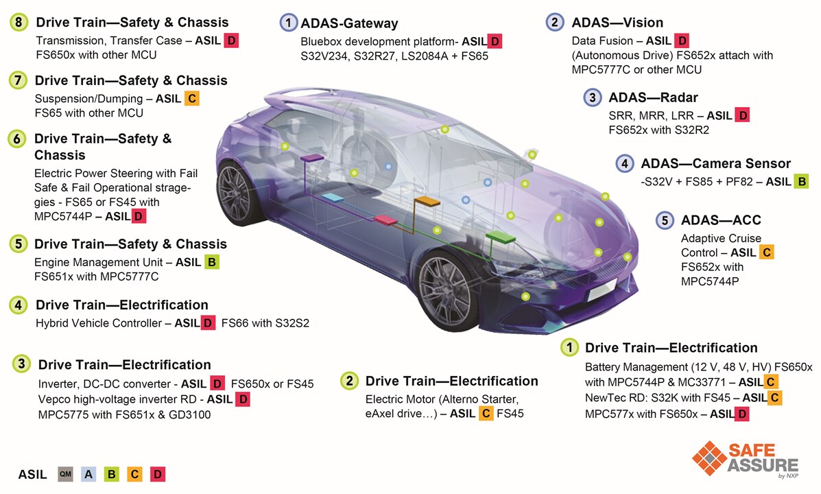
Safe Assure® (Functional Safety)
When it comes to functional safety, NXP stands for quality and reliability. Our SafeAssure program simplifies system-level safety requirements in accordance with ISO 26262.
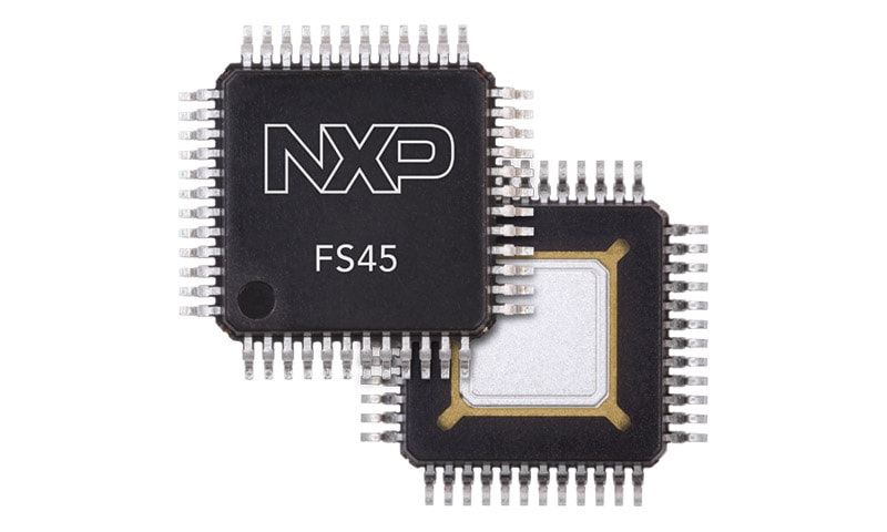
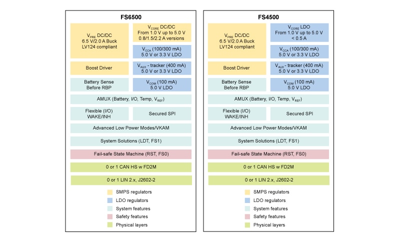
The FS45 system basis chip (SBC) provides power to MCUs and optimizes energy consumption through a DC/DC pre-regulator and linear regulators and ultra-low-power saving modes. Featuring:
| Part Number | FS1B [1] | LDT [2] | CAN | LIN | Preferred superset PN w/ Linear VCORE | Preferred superset PN w/ DC-DC VCORE |
|---|---|---|---|---|---|---|
| FS45/FS65x5NAE | No | No | No | No | FS4507L or FS4508C | FS6527L or FS6528C |
| FS45/FS65x5CAE | No | No | Yes | No | FS4507L or FS4508C | FS6527L or FS6528C |
| FS45/FS65x5KAE | No | No | No | Yes | FS4507L | FS6527L |
| FS45/FS65x5LAE | No | No | Yes | Yes | FS4507L | FS6527L |
| FS45/FS65x6NAE | Yes | No | No | No | FS4508C | FS6528C |
| FS45/FS65x6CAE | Yes | No | Yes | No | FS4508C | FS6528C |
| FS45/FS65x7NAE | No | Yes | No | No | FS4507L or FS4508C | FS6527L or FS6528C |
| FS45/FS65x7CAE | No | Yes | Yes | No | FS4507L or FS4508C | FS6527L or FS6528C |
| FS45/FS65x7KAE | No | Yes | No | Yes | FS4507L | FS6527L |
| FS45/FS65x7LAE | No | Yes | Yes | Yes | FS4507L | FS6527L |
| FS45/FS65x8NAE | Yes | Yes | No | No | FS4508C | FS6528C |
| FS45/FS65x8CAE | Yes | Yes | Yes | No | FS4508C | FS6528C |
| Part Number | FS1B [1] | LDT [2] | VKAM On | CAN | LIN | Preferred superset PN w/ Linear VCORE | Preferred superset PN w/DC-DC VCORE |
|---|---|---|---|---|---|---|---|
| FS45/FS65x0NAE | No | No | by SPI | No | No | MC33FS4502LAE | MC33FS6522LAE |
| FS45/FS65x0CAE | No | No | by SPI | Yes | No | ||
| FS45/FS65xOLAE | No | No | by SPI | Yes | Yes | ||
| FS45/FS65x1NAE | Yes | No | by SPI | No | No | MC33FS4503CAE | MC33FS6523CAE |
| FS45/FS65x1CAE | Yes | No | by SPI | Yes | No | ||
| FS45/FS65x2NAE | No | Yes | by SPI | No | No | MC33FS4502LAE | MC33FS6522LAE |
| FS45/FS65x2CAE | No | Yes | by SPI | Yes | No | ||
| FS45/FS65x2LAE | No | Yes | by SPI | Yes | Yes | ||
| FS45/FS65x3NAE | Yes | Yes | by SPI | No | No | MC33FS4503CAE | MC33FS6523CAE |
| FS45/FS65x3CAE | Yes | Yes | by SPI | Yes | No | ||
| FS65x4LAE | No | Yes | by default | Yes | Yes | - | MC33FS6524LAE |
When it comes to functional safety, NXP stands for quality and reliability. Our SafeAssure program simplifies system-level safety requirements in accordance with ISO 26262.
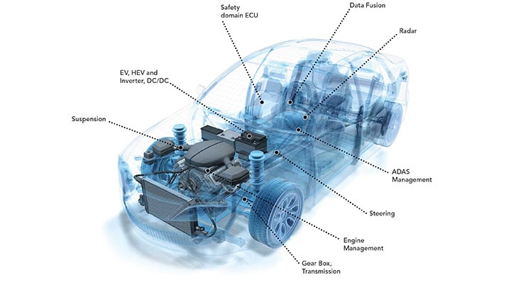
This platform facilitates the design of safe power management systems thanks to a portfolio of configurable and linkable devices. It simplifies complex power supply subsystems into a single smart solution.
Participating products are available for a minimum of 10 years. Designated participating products developed for the automotive, telecom and medical segments are available for a minimum of 15 years.
|
|
|
|
|
|
|
|---|---|---|---|---|---|
|
|
|
|
|
|
|
|
|
|
|
|
|
|
|
|
|
|
|
|
|
|
|
|
|
|
|
|
|
|
|
|
|
|
|
|
|
|
|
|
|
|
|
|
|
|
|
|
|
|
|
|
|
|
|
|
|
|
|
|
|
|
|
|
|
|
|
|
|
|
Quick reference to our documentation types
1-10 of 14 documents
Compact List
1 design file
Receive the full breakdown. See the product footprint and more in the eCad file.
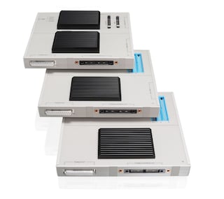
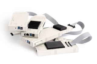
4 hardware offerings
Additional hardware available. View our featured partner solutions.
Quick reference to our software types.
2 software files
Note: For better experience, software downloads are recommended on desktop.
To get further assistance directly from NXP, please see our Engineering Services.
1 engineering service

To find additional partner offerings that support this product, visit our Partner Marketplace.