
Layerscape® 1043A and 1023A Processors
The Layerscape® Access LA9310 programmable baseband processor is a digital signal processor with integrated data converters (ADC/DAC) for physical layer processing of 5G infrastructure, DFE, and custom communication systems at the network edge. Its low cost and power and programmable signal processing capabilities make it an attractive option to expensive FPGAs in applications such as network listening, small-scale radio units and repeaters.
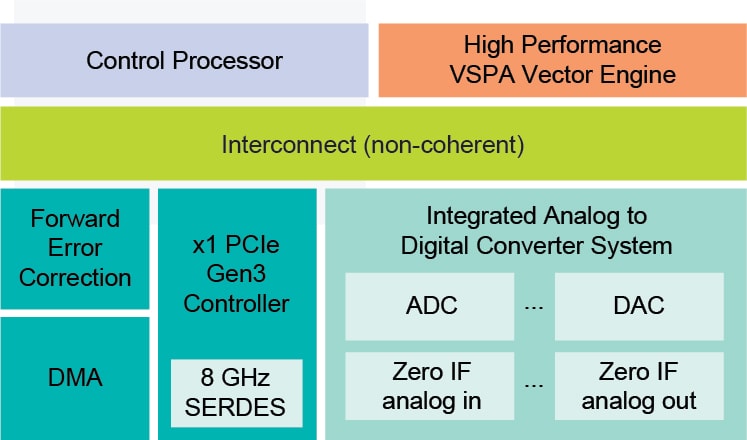
The ADC / DAC supports a zero-IF I/Q interface to an RFIC suitable for both sub-6GHz and limited bandwidth mmWave applications. NXP’s VSPA DSP implements sample-level baseband processing in the digital domain, enabling a flexible software defined radio.
The ADC / DAC analog subsystem supports a zero-IF I/Q interface toward an RFIC. With a sample rate of up to 153M samples per second, is suitable for both sub-6GHz and limited bandwidth mmWave applications. The Vector Signal Processing Accelerator (VSPA) DSP leverages NXP supplied software libraries to efficiently implement sample-level baseband processing in the digital domain (that is, digital up/down conversion, digital filtering, et cetera), enabling a flexible software defined radio for standard and proprietary protocols. Results are provided to the host, typically an LS1023A or LS1043A, over a x1 Gen3 PCIe interface. The device includes DMA engines, timing blocks and RF control interfaces such as I²C, SPI and proprietary LLCP signaling.
In addition, the LA9310 is intended for use in industrial and measurement use-cases. For such applications, the LA9310 functions as a lookaside accelerator to a host processor such as the i.MX family of devices, functioning as a signal preprocessor that includes analog sample acquisition together with initial DSP (filter/data reduction) processing, or as a math accelerator. In these use-cases, the lookaside accelerator often replaces an FPGA, connecting over PCIe or Ethernet.
NXP provides a BSP for the LA9310 that includes drivers for all chip capabilities, example hello-world application that exercise the full data path of the device, VSPA libraries and FreeRTOS running on the M4 core. Reference code for target applications is available.
CodeWarrior for VSPA enables users to compile and debug VSPA code.
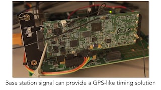
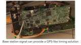
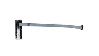
The LA9310 Reference Design Kit is a standalone system that consists of an LA9310 daughter card plugged into an LS1043A Reference Design Board. Customers can copy its design, use it to evaluate performance, and use it to debug their own hardware.
|
|
|
|
|
|
|
|---|---|---|---|---|---|
|
|
|
|
|
|
|
|
|
|
|
|
|
|
|
|
|
|
|
|
|
|
|
|
|
|
|
|
|
|
|
|
|
|
|
|
|
|
|
|
|
|
|
|
|
|
|
|
|
|
|
|
|
|
|
|
|
|
|
|
|
|
|
|
|
|
|
|
|
|
Quick reference to our documentation types
1-10 of 15 documents
Compact List
Receive the full breakdown. See the product footprint and more in the eCad file.
1 hardware offering
Quick reference to our software types.
3 software files
Note: For better experience, software downloads are recommended on desktop.
To get further assistance directly from NXP, please see our Engineering Services.
1-5 of 12 engineering services

To find additional partner offerings that support this product, visit our Partner Marketplace.