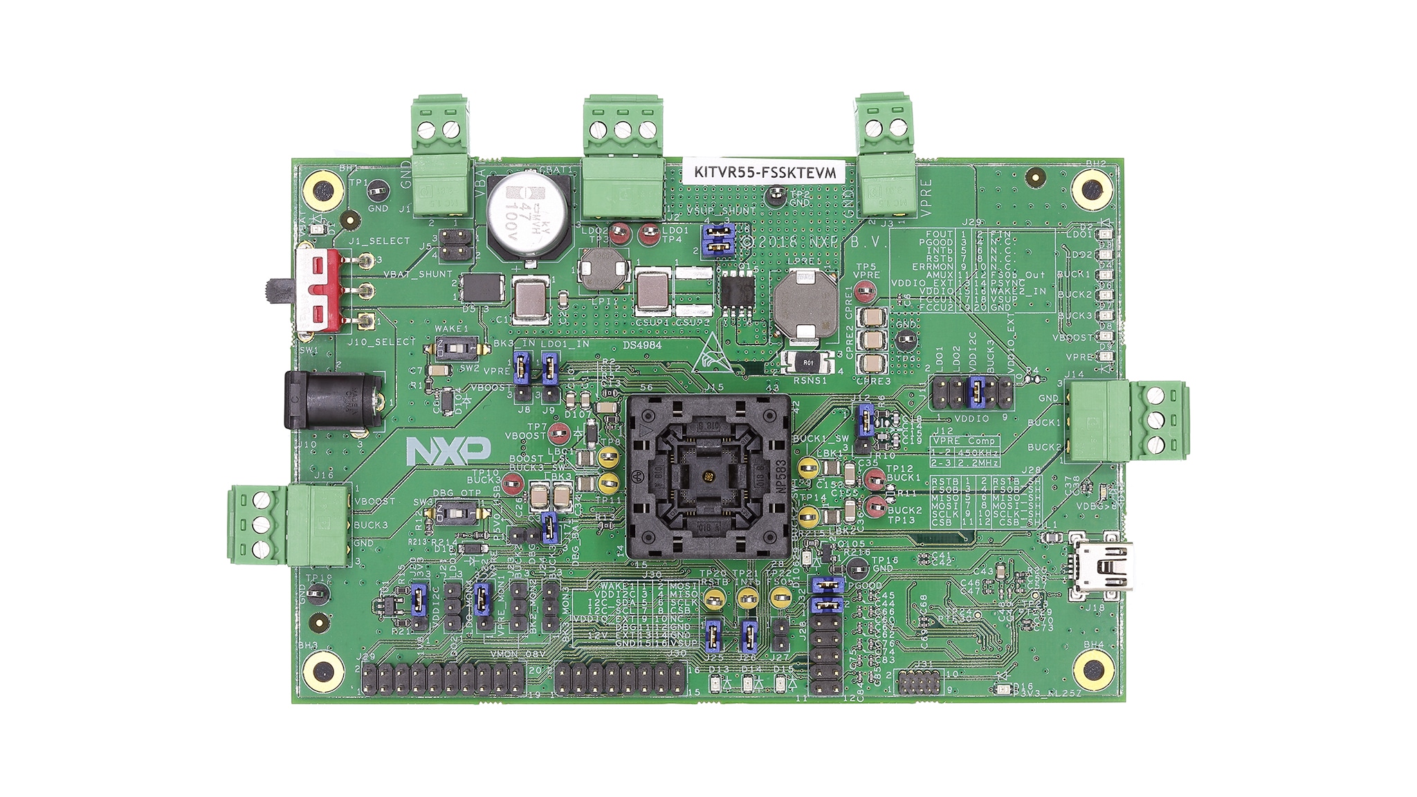
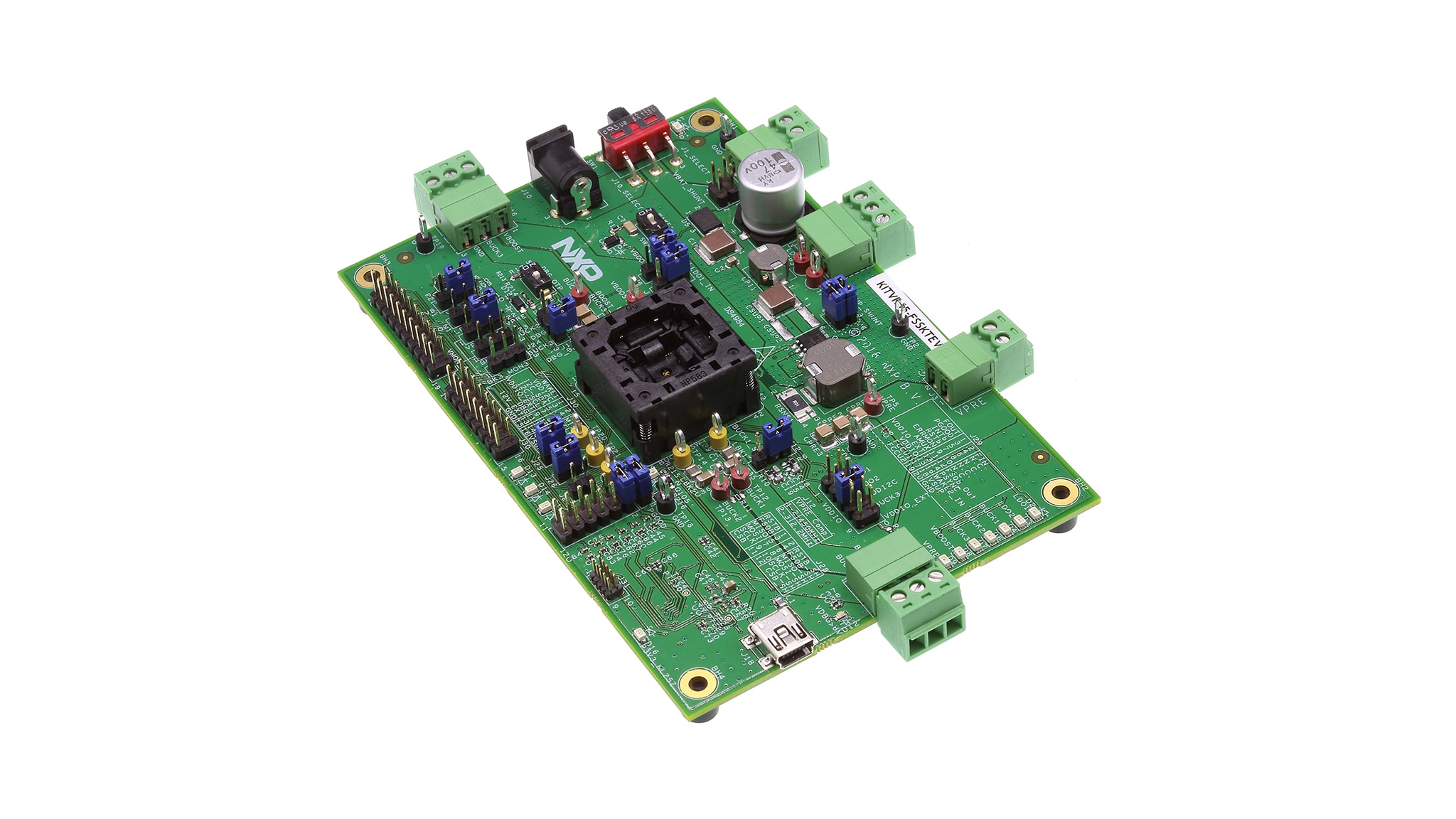
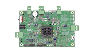
VR5500 Safety SBC Programming Board

KITVR55-FSSKTEVM

Roll over image to zoom in

Block Diagram

VR5500, High Voltage PMIC Block Diagram

VR5500, High Voltage PMIC Block Diagram

Supported Devices

Power Management

System Basis Chips

Features

General specifications

  • VBAT power supply connectors (Jack and Phoenix)
  • VPRE output 3.3 V/ 3.8 V/ 4.1 V/ 5.0 V
  • VBUCK1/2 in a standalone or multi-phase mode
  • VBUCK3
  • VBOOST 5.0 V or 5.74 V, up to 800 mA
  • LDO1 and LDO2, from 1.1 V to 5 V, up to 400 mA
  • Ignition key switch
  • Embedded USB connection for easy connection to software GUI (access to I2C bus, IOs, RSTB, INTB, Debug, MUX_OUT, regulators)
  • LEDs that indicate signal or regulatory status
  • Support OTP fuse capabilities
  • USB connection for register access, OTP emulation and fuse
  • Note that due to the socket, all output current should be limited to 1 A maximum

Buy Options

KITVR55-FSSKTEVM-Image

Click to expand

  • KITVR55-FSSKTEVM

  • VR5500 Safety SBC Programming Board.

  • $433.25 USD
  • For a quantity of 1
    • Availability: In stock
    • Inventory: 5
    • Shipping: Normally ships 1-2 business days
Buy from NXPBuy From Distributor

Documentation

Quick reference to our documentation types.

3 documents

Design Resources

Design Files

2 design files

Software

1 software file

Note: For better experience, software downloads are recommended on desktop.

Support

What do you need help with?