Design Files
2 design files
-
Printed Circuit Boards and Schematics
Coin Cell Hardware Design Files.
-
Design Files - miscellaneous
JN-RD-6054-JN5189 Design Files
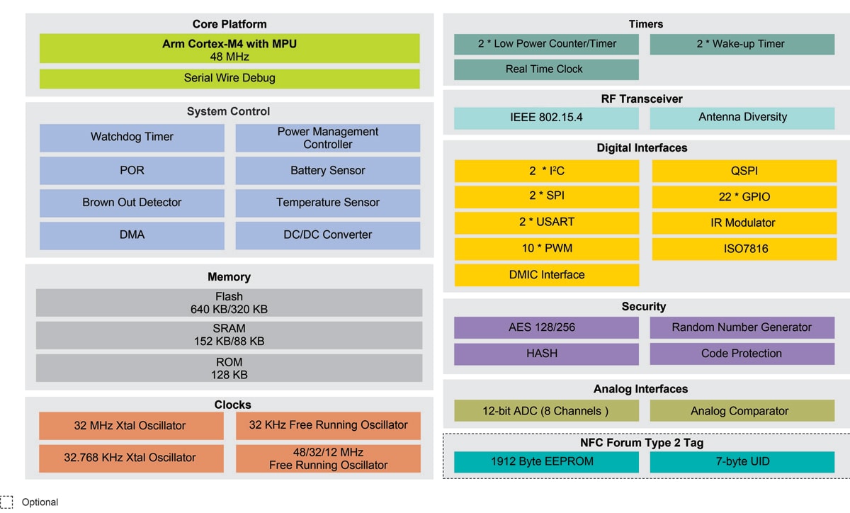
The JN5189 portfolio is designed to power the next generation of very low current wireless devices, supporting Zigbee 3.0, Thread, and IEEE 802.15.4. It includes several low-power modes and ultra-low TX and RX power consumption, which enables devices powered by JN5189/88 to have a longer battery life. With -100 dBm RX sensitivity and up to +11 dBm TX output power, JN5189/88 offers reliable and robust communications performance.JN5189/88 is powered by an Arm® Cortex®-M4 MCU and can run up to 640 KB onboard flash and 152 KB SRAM, with enough room and flexibility for complex applications and OTA upgrade capability without external memory. It has a rich set of MCU peripherals and multiple serial communication interfaces for embedded connected applications. JN5189T/88T has an integrated NFC NTAG to implement contactless NFC commissioning, simplifying the network build-out.
Part numbers include: JN5188HN, JN5188THN, JN5189HN, JN5189THN.
Quick reference to our documentation types.
1-5 of 27 documents
2 design files
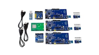
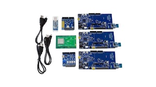
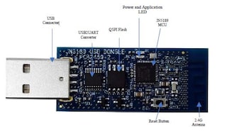
1-5 of 8 hardware offerings
Additional hardware available. View our featured partner solutions.
1-5 of 9 software files
Additional software available. View our featured partner solutions.
Note: For better experience, software downloads are recommended on desktop.