Getting Started with the KIT6X02AS2T1
Contents of this document
-
Out of the Box
-
Get to Know Hardware
-
Configure Hardware
Sign in to save your progress. Don't have an account? Create one.
Purchase your Evaluation Board for BMA6X02 with SPI
1. Out of the Box
This page guides you through the process of setting up and using the KIT6X02AS2T1 board.
1.1 Kit Contents and Packing List
The KIT6X02AS2T1 includes:
- KIT6X02AS2T1: SPI2TPL evaluation board for BMA6X02 with serial peripheral interface (SPI) and transport
- Protocol link (TPL) communication
- Cable for supply
- Electrical transport protocol link (ETPL) cable, which is a two-wire twisted pair TPL cable (50 cm)
2. Get to Know Hardware
The purpose of the KIT6X02AS2T1 is to allow a communication of a standard microcontroller (MCU) with NXP analog front-end (AFE) boards (for example, EVBMA7X18DT1 or EVBMA777T3).
2.1 Board Features
The main features of the KIT6X02AS2T1 are:
- Communication link from SPI to TPL and back
- Configuration options for the different SPI modes offered by the BMX6X02AS
- Configuration options for the different clock modes offered by the BMX6X02AS
- Configuration options for different supply concepts
- Easy access to the serial peripheral interface (SPI) communication lines
- Two galvanically isolated ETPL ports
- Support for the transformer physical layer 3 (TPL3) protocol version
- Three status LEDs
2.2 Board Description
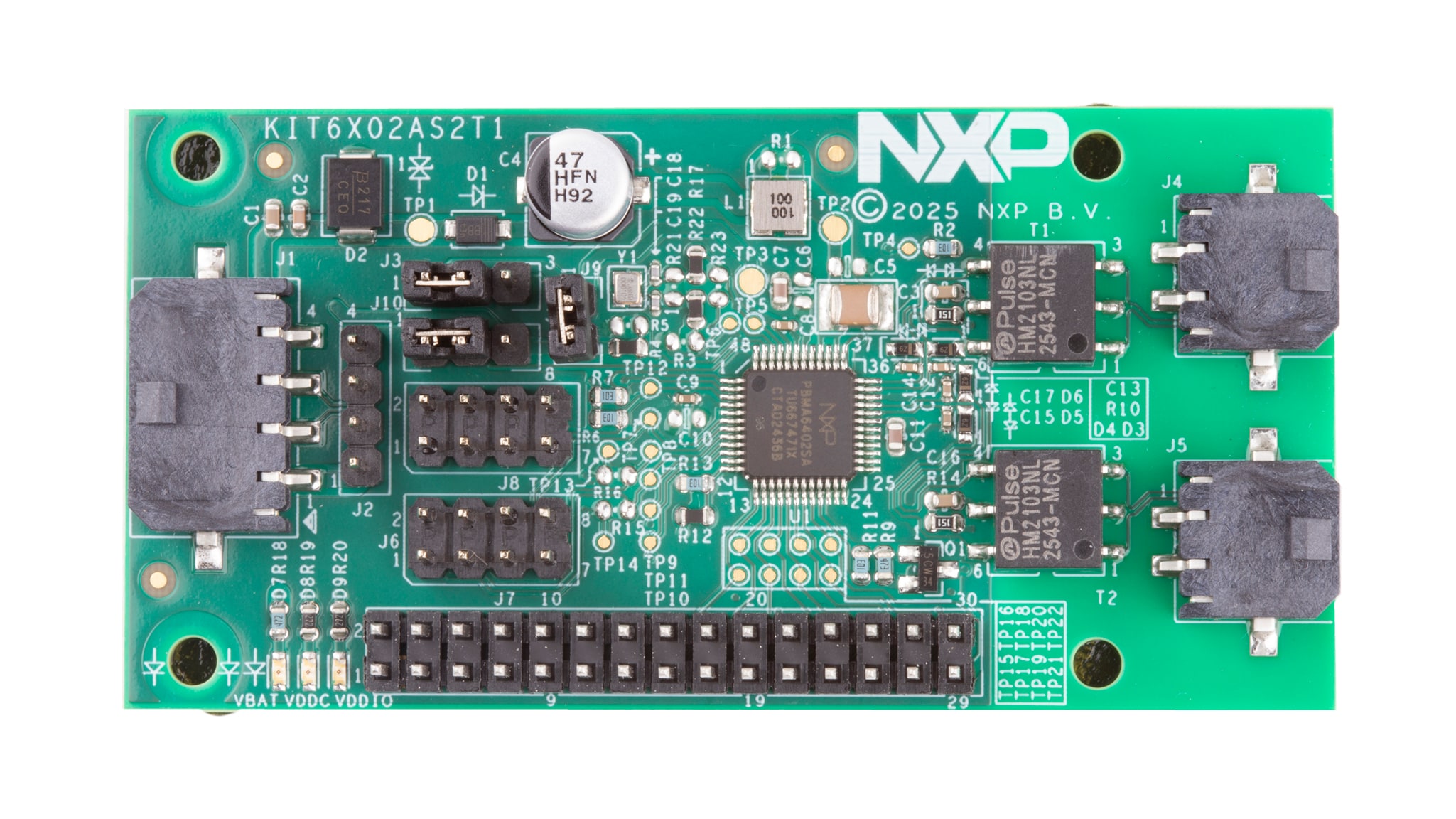
The KIT6X02AS2T1 is an evaluation board designed for the BMX6X02 general-purpose battery management system (BMS) communication gateway and electrochemical impedance spectroscopy (EIS) synchronization controller (see Figure 1). It is equipped with a BMA6402AS device, which integrates the synchronization functionality required for EIS measurements. The BMA6402AS combines the full feature sets of the BMA6002AS, BMI6402AS and BMI6002AS, enabling the KIT6X02AS2T1 board to function as a versatile evaluation platform for all associated device variants.

3. Configure Hardware
The KIT6X02AS2T1 has several configuration options. The most important ones are the clock and supply configuration (see Section 3.2) and the MCU interface (see Section 3.1).
3.1 MCU Interface
The MCU interface (see Figure 2) of the KIT6X02AS2T1 allows the connection toward the MCU.

All relevant pins of the BMX6X02 are routed to the MCU interface, enabling flexible and application-specific MCU connections, such as single SPI or dual SPI configurations. Because SPI signals typically operate at high frequencies, each SPI line is paired with an adjacent ground (GND) pin to ensure signal integrity and minimize noise. The connector pin assignments are listed in Table 1. With the board dual and single SPI operation can be achieved. For single SPI configuration, the SPI clock and the chip select pins must be connected. This connection can be achieved by an appropriate external wiring or by population of R15 and R16.
| Pin number | Function | Description |
|---|---|---|
| 1 | VSS | ground as reference |
| 2 | CSN_RSP | 1. Target response SPI chip select input 2. Controller response SPI chip select output |
| 3 | VSS | ground as reference |
| 4 | SCLK_RSP | 1. Target response SPI clock input 2. Controller response SPI clock output |
| 5 | VSS | ground as reference |
| 6 | SDAT_RSP_TXD | response SPI data output |
| 7 | VSS | ground as reference |
| 8 | CSN_REQ | request SPI chip select input |
| 9 | VSS | ground as reference |
| 10 | SCLK_REQ | request SPI clock input |
| 11 | VSS | ground as reference |
| 12 | SDAT_REQ_RXD | request SPI data input |
| 13 | VSS | ground as reference |
| 14 | OSCP | external clock positive input |
| 15 | GPIO0 | 1. General-purpose input 0 2. General-purpose output 0 3. Interrupt 0 output (INT0) |
| 16 | VSS | ground as reference |
| 17 | GPIO1 | 1. General-purpose input 1 2. General-purpose output 1 3. Interrupt 1 output (INT1) 4. CSN3 for peripheral SPI controller |
| 18 | STB_N_OUT | standby output, active LOW |
| 19 | GPIO2 | 1. General-purpose input 2 2. General-purpose output 2 3. Interrupt 2 output (INT2) 4. CSN2 for peripheral SPI controller |
| 20 | STB_OUT | standby output, active HIGH |
| 21 | GPIO3 | 1. General-purpose input 3 2. General-purpose output 3 3. Interrupt 3 output (INT3) 4. CSN1 for peripheral SPI controller |
| 22 | TPL_WAKE | wake output of the evaluation board (EVB) for waking up of the system |
| 23 | GPIO4 | 1. General-purpose input 4 2. General-purpose output 4 3. I²C bus SCL 4. SCLK for peripheral SPI controller |
| 24 | RESET | reset input of BMX6X02 |
| 25 | GPIO5 | 1. General-purpose input 5 2. General-purpose output 5 3. I²C bus SDA 4. Controller output target input (COTI) for peripheral SPI controller |
| 26 | VSS | ground as reference |
| 27 | GPIO6 | 1. General-purpose input 6 2. General-purpose output 6 3. Synchronization input 4. CSN0 for peripheral SPI controller |
| 28 | VEXT | external supply voltage for VDDIO |
| 29 | GPIO7 | 1. General-purpose input 7 2. General-purpose output 7 3. Hold input 4. Controller input target output (CITO) for peripheral SPI controller |
| 30 | VSS | ground as reference |
3.2 Jumpers
The KIT6X02AS2T1 has three jumpers for the supply and clock selection (see Figure 3).

The supply jumpers can be used to realize different supply and clock concepts.
3.3 Supply Options
J3 (marked red) is used to select the voltage digital drain input/output (VDDIO) supply voltage.
- When the jumper is placed in position 1-2, the VDDIO voltage is sourced from voltage regulator (VREG), the internal 5 V regulator of the BMX6X02S.
- When the jumper is placed in position 2-3, the VDDIO voltage is sourced from voltage external (VEXT). An external VEXT supply can be provided through connector
J7, pin 29.
J9 (marked blue) is used to select the voltage digital core (VDDC) voltage for the BMX6X02S
- When the jumper is placed in position 1-2, the VDDC voltage is is sourced from VREG, the internal 5 V regulator of the BMX6X02S.
- Alternative 5 V sources can be directly applied to
J9, pin 2.
3.4 Clock Options
The BMX6X02S supports multiple clock source configurations (marked orange). By default, the device uses the external oscillator mounted on the KIT6X02AS2T1, providing a robust and stable reference suitable for EIS measurements.
To reduce system cost, the MCU may alternatively provide the clock signal through one of its general-purpose input/output (GPIO) pins. Because this signal operates at a high frequency, maintaining good signal integrity can be challenging. If the clock line is shielded and kept shorter than 10 cm, acceptable performance can still be achieved. For this configuration, inject the clock signal into J9, pin 14, remove the 0 Ω resistors at R17 and R22 and install one of them at R23, leaving R3 unpopulated. If EIS functionality is not required, the BMX6X02S can operate using its internal clock source. To enable the internal clock, place jumper J1 in position 2-3.
Design Resources
Board Information
Additional References
In addition to our KIT6X02AS2T1 page, you may also want to visit: