
Automotive Tiny Real-Time Clock/Calendar with Alarm Function and I²C-Bus
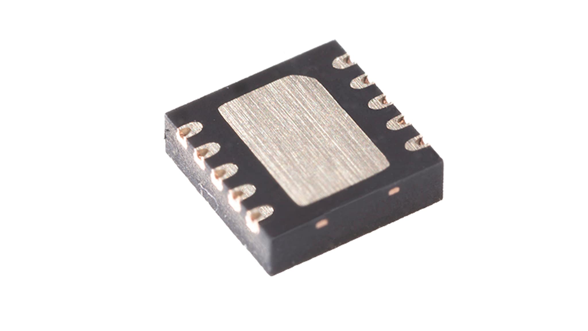
The PCA8525TK/Q900 is a real-time clock (RTC) integrated circuit (IC) with integrated temperature compensation that improves timekeeping accuracy to ±30 ppm, delivering up to 5x better performance than current market offerings. It supports temperature ratings up to 125 °C and is available in an HVSON10 package option.
Automotive Tiny Real-Time Clock/Calendar with Alarm Function and I²C-Bus
Quick reference to our documentation types
3 documents
Compact List