Product Longevity
Participating products are available for a minimum of 10 years. Designated participating products developed for the automotive, telecom and medical segments are available for a minimum of 15 years.
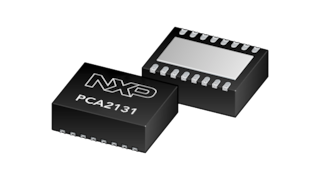
The PCA85074ADP is a Real-Time Clock (RTC) and calendar optimized for low power consumption and operating temperature up to 125 °C. An offset register allows fine tuning of the clock. All addresses and data are transferred serially via the two-line bidirectional I²C-bus. The maximum data rate is 400 kbit/s. The register address is incremented automatically after each written or read data byte.
Choose a diagram:
Participating products are available for a minimum of 10 years. Designated participating products developed for the automotive, telecom and medical segments are available for a minimum of 15 years.
|
|
|
|
|
|
|
|---|---|---|---|---|---|
|
|
|
|
|
|
|
|
|
|
|
|
|
|
|
|
|
|
|
|
|
|
|
|
|
|
|
|
|
|
|
|
|
|
|
|
|
|
|
|
|
|
|
|
|
|
|
|
|
|
|
|
|
|
|
|
|
|
|
|
|
|
|
|
|
|
|
|
|
|
Quick reference to our documentation types
3 documents
Compact List
Receive the full breakdown. See the product footprint and more in the eCad file.