


MCX A17: Essential Arm® Cortex® M33 MCU with 180 MHz and Rich Serial Peripherals
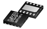
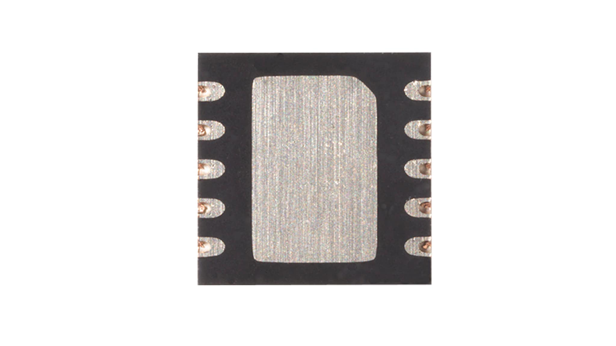
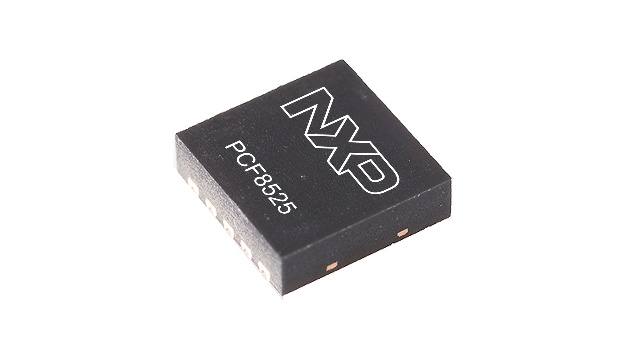
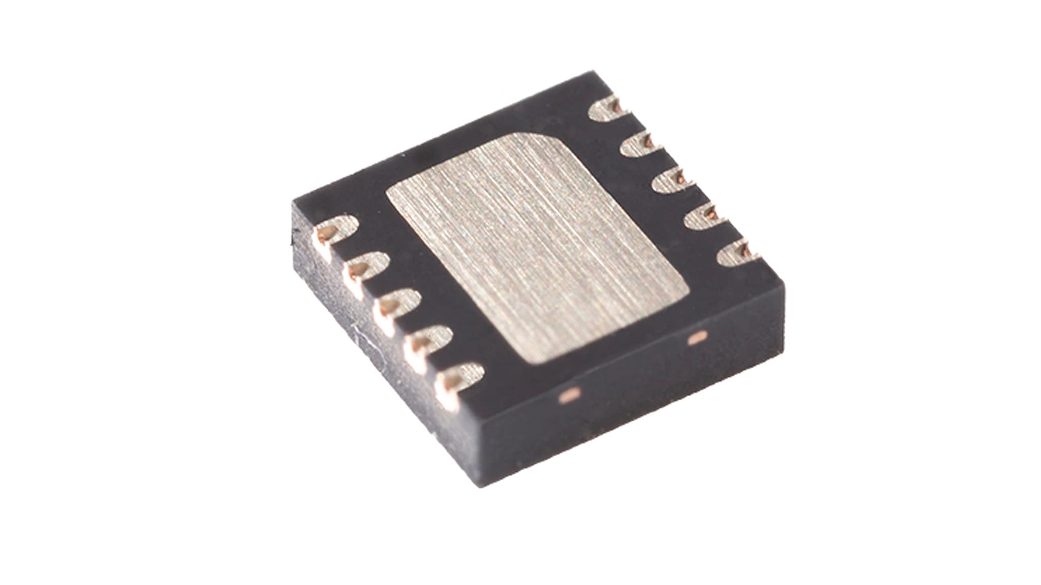
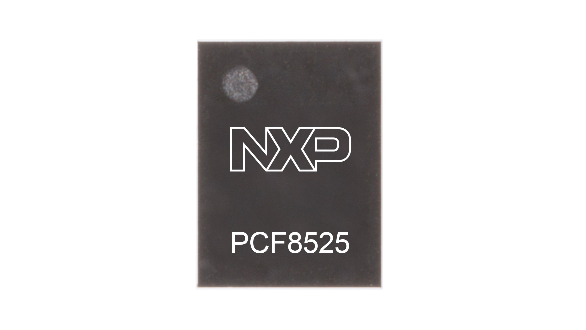
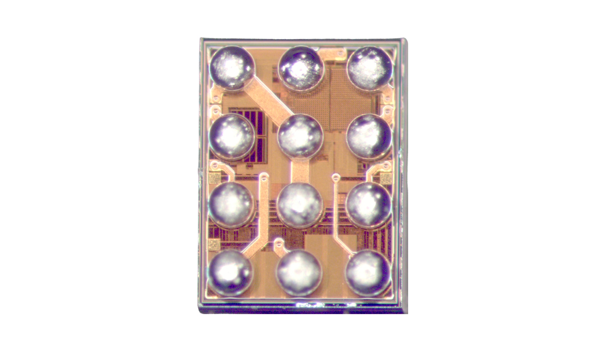
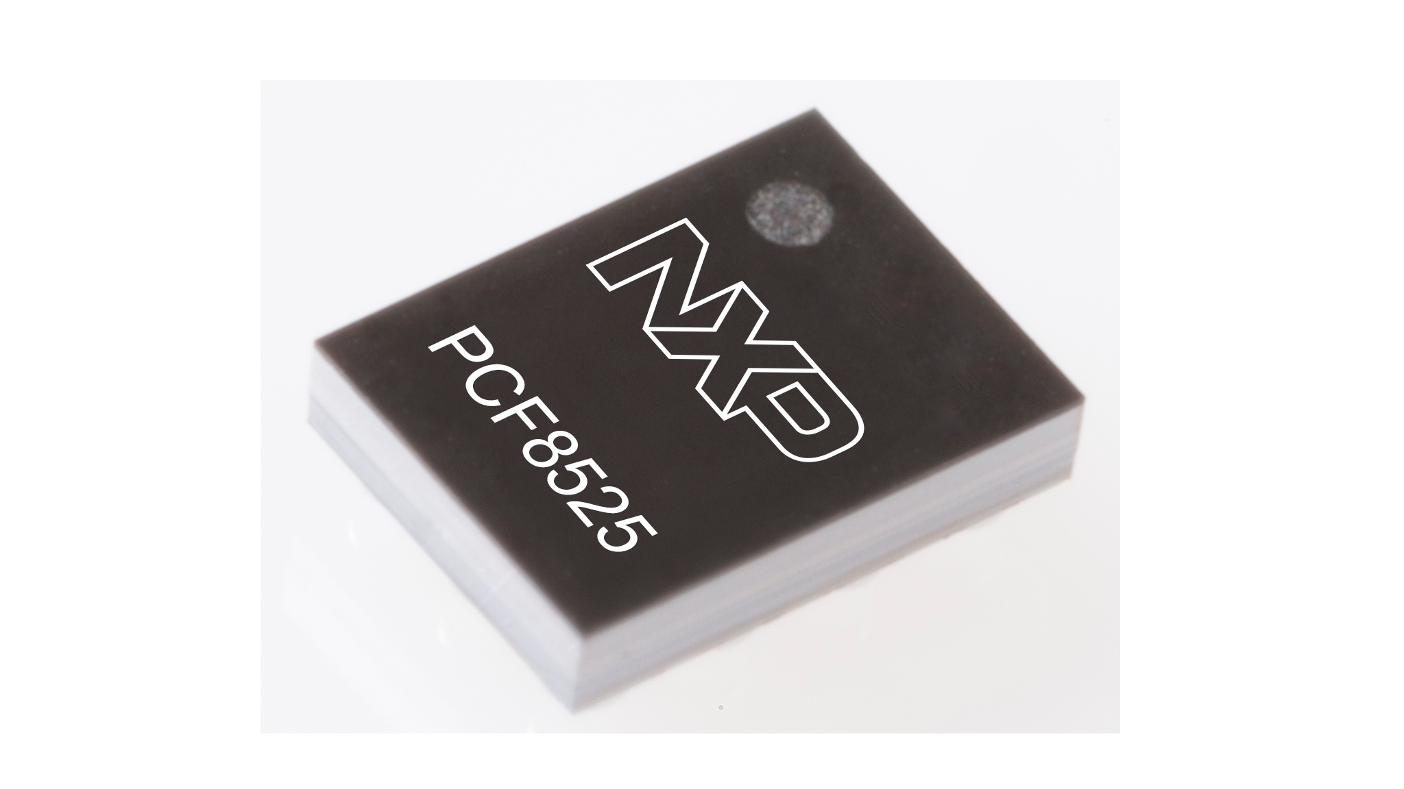
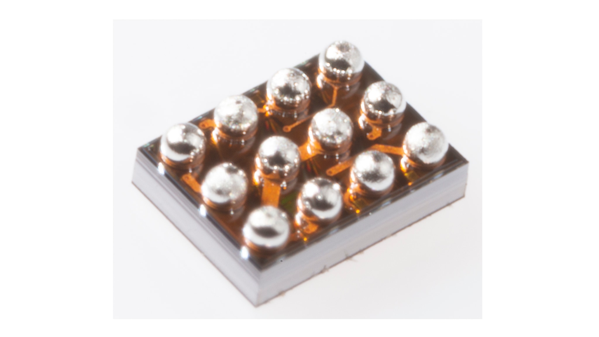
The PCF8525 is a real-time clock (RTC) integrated circuit (IC) offering accurate timekeeping performance. The HVSON version includes temperature compensation for up to ±30 ppm accuracy, delivering up to 5x better than other RTC IC solutions, while the WLCSP variant omits compensation to achieve an ultra-compact footprint for space-constrained designs.
Quick reference to our documentation types
4 documents
Compact List