Product Longevity
Participating products are available for a minimum of 10 years. Designated participating products developed for the automotive, telecom and medical segments are available for a minimum of 15 years.
The P3A9606JK is a 2-bit, dual supply translating transceiver with auto direction sensing, that enables bidirectional voltage level translation for traditional open drain I²C-bus/SMBus applications, combination open drain and push pull 12.5 MHz I3C-bus applications or push pull SPI applications (with two devices).
Both VCC(A) and VCC(B) can be supplied at any voltage between 0.72 V and 1.98 V making the device suitable for translating between any of the low voltage nodes (0.8 V, 1.2 V and 1.8 V).
It features two 1-bit input-output ports (An and Bn) controlled by one output enable input (OE).
| Part Number | VCC(A) | VCC(B) | Signal |
| PCA9306 | 1 to 3.6 V | 2 to 5.5 V | I²C |
| NTB0104 | 1.2 to 3.6 V | 1.65 to 5.5 V | SPI |
| P3A9606 | 0.72 to 1.98 V | 0.72 to 1.98 V | I²C, SPI or I3C |

Participating products are available for a minimum of 10 years. Designated participating products developed for the automotive, telecom and medical segments are available for a minimum of 15 years.

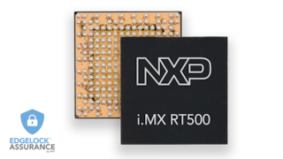
i.MX RT500 Crossover MCU with Arm® Cortex®-M33, DSP and GPU Cores

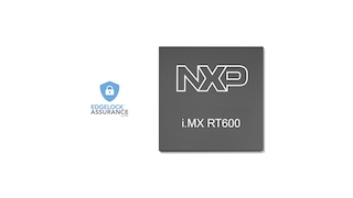
i.MX RT600 Crossover MCU with Arm® Cortex®-M33 and DSP Cores
|
|
|
|
|
|
|
|---|---|---|---|---|---|
|
|
|
|
|
|
|
|
|
|
|
|
|
|
|
|
|
|
|
|
|
|
|
|
|
|
|
|
|
|
|
|
|
|
|
|
|
|
|
|
|
|
|
|
|
|
|
|
|
|
|
|
|
|
|
|
|
|
|
|
|
|
|
|
|
|
|
|
|
|
Quick reference to our documentation types
6 documents
Compact List
Please wait while your secure files are loading.
1 design file
Receive the full breakdown. See the product footprint and more in the eCad file.
Please wait while your secure files are loading.