

Hardware
1 hardware offering
-
 Evaluation and Development Boards
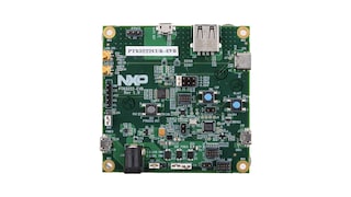
PTN3222CUK-EVB eUSB2 to USB2 Redriver Evaluation Board
The PTN3222 device family is a set of 1-port eUSB2 to USB2 redrivers, enabling advanced process node SoCs to connect with traditional legacy USB2 interface. Family offers a variety of devices with different features to fit into the different SoCs available on the market. For more information about the family features options, please check the summary table below.
Choose a diagram:
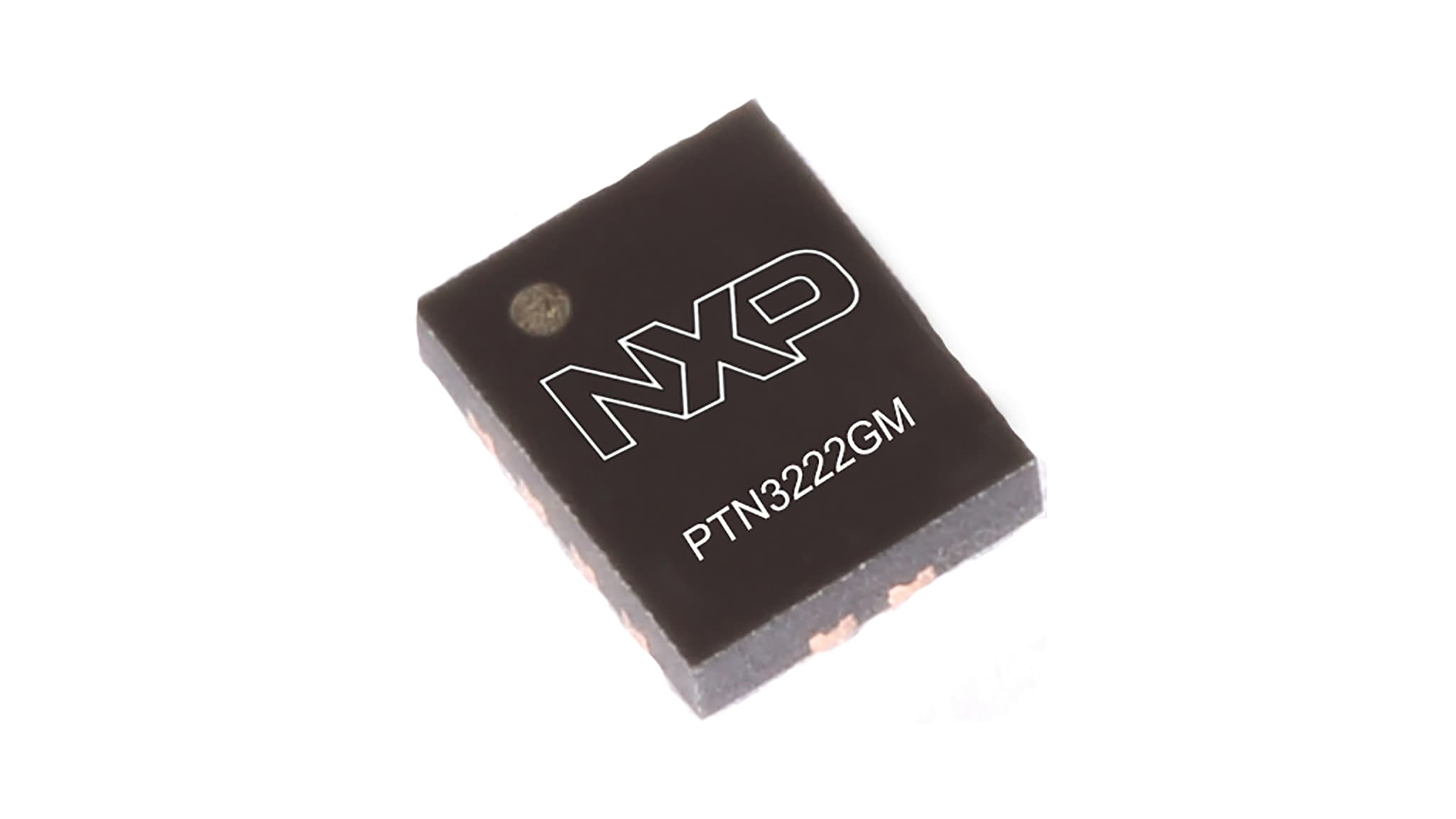
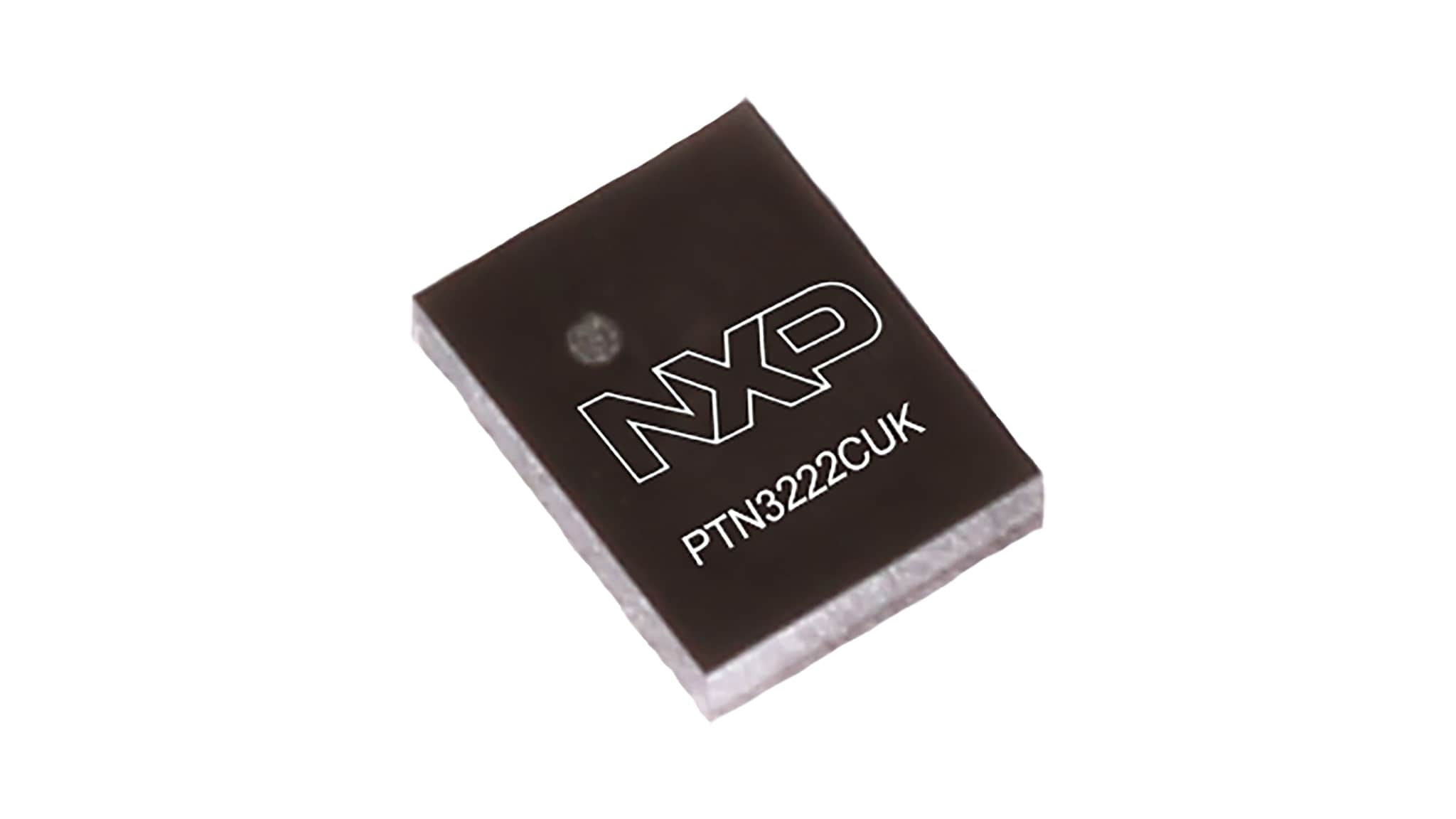
Part numbers include: PTN3222CUK, PTN3222DUK, PTN3222EUK, PTN3222GM.
| Device | Package | Status | I/O VDD (*1) | Comments |
|---|---|---|---|---|
| PTN3222CUK | WLCSP12 | Production | 1.8 V | General market |
| PTN3222DUK | WLCSP12 | Production | 1.8 V | Recommend for Qualcomm platforms (*2) |
| PTN3222EUK | WLCSP12 | Production | 1.2 V | General market |
| PTN3222GM | QFN12 | Production | 1.8 V | General market |
| PTN3222DHN | QFN12 (*3) | Development (*4) | 1.8 V | Automotive version |
Quick reference to our documentation types.
1-5 of 6 documents
1 hardware offering
To get further assistance directly from NXP, please see our Engineering Services.
1 engineering service
To find a complete list of our partners that support this product, please see our Partner Marketplace.