
Ultra-Low-Power, Highly Integrated MCU
Design Files
Quick reference to our
design files types.
2 design files
Receive the full breakdown. See the product footprint and more in the eCad file.
-
Models
IBIS files for LPC51U68
-
Printed Circuit Boards and Schematics
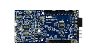
LPCXpresso51U68 development board (OM40005) schematic (PDF), BOM and Gerber files.