Ready for the rising tide of 5G rollouts, NXP has a set of programmable baseband processors for the 5G access edge. With programmability comes flexibility, enabling these chips to support evolving standards and deployment models while facilitating interoperability. These new
Layerscape®
Access processors extend the trail blazed by our
Layerscape Access LA1575
device.
Two and a half years ago the
then-new processor.
This first Layerscape Access processor still seeks to revolutionize network economics by lengthening hardware lifecycles by enabling incremental upgrades via software. To this end, its key feature is programmability in three domains: application, Layer 2 and physical layer. This chip has generated interest from companies developing both wired and wireless systems. After all, communications technologies from phoneline-based G.Fast to wireless 5G all rely on OFDM at the physical layer. For production, however, customers need processors pared to their requirements to cut cost.
We’re, therefore, pleased to introduce our new Layerscape Access processors, the LA9350, LA9310 and
LA12xx
families. Like the LA1575, these new devices have programmable PHYs and control functions. Unlike their predecessor, they leave application processing to external hosts, such as Layerscape LS1 or LS2 processors. Diverse systems can use these programmable processors. Some of our most exciting targets are in 5G access.
Delivering a Programmable Baseband for Open, Intelligent 5G
The 5G era ushers in a few changes to the industry as a whole and to the radio access network (RAN). Driving industry change is the O-RAN Alliance, a group formed by operators focused on openness and intelligence in 5G technology. The aim of openness is to foster networks made of interoperable equipment from multiple vendors. Although telecommunications technology is standardized, standards leave enough room for interpretation that service providers have conventionally used the same vendor throughout the RAN in a region to avoid compatibility problems. The alliance endeavors to mix and match equipment and to replace vendor-proprietary hardware with generic equivalents. The not-too-subtle goal is to reduce their capital expenses for upgrading to 5G.
Intelligence is about reducing operating expenses. Wireless networks are becoming more complex, adding cell sites and serving broader needs. With added smarts, the network can allocate radio resources and otherwise manage its own operation. Equipment, therefore, must be flexible. It also must be programmable to run the software that imbues it with intelligence.
The O-RAN Alliance is also contributing to changes in the RAN’s structure. The 5G standard takes the unusual approach of defining not just a single system to implement baseband functions but instead eight different ways to logically split up these functions. The alliance bases their reference architecture on the approach where a radio unit (RU) implements RF transceiver and lower-level baseband PHY functions, a distributed unit (DU) performs upper-level PHY and media access functions and a central unit (CU) executes higher-layer protocols, with the user and control planes logically separated in the CU. A critical challenge is that the DU and CU are to have characteristics of both standard Linux® computers and real-time systems. Furthermore, although the three units are logically separate, they may be physically combined in different permutations. All three could be in the same system as in a traditional base station, the RU and DU can be merged, one DU can serve multiple RU, the CU can be a standalone system or the CU can be a virtual machine in a distant data center, for example. Such diversity further justifies an open, flexible approach.
Other structural RAN changes include embracing massive MIMO (64 or more transmitters and receivers) and what I’ll call medium MIMO (16 or so transmitters and receivers)—both of which requires additional processing in the RU compared with lower-radix MIMO—and opening up the 24 GHz-100 GHz millimeter wave (mmWave) bands which shrinks cell size owing to their poor propagation. Service providers are also taking advantage of 5G’s faster speeds to market it as an alternative to wireline broadband, requiring new fixed-wireless access (FWA) premises equipment. There’s also talk of private 5G networks using 5G technology as an enterprise-operated LAN. Operators also perennially worry about whether consumers’ home networks adequately convey to personal devices the data the operator delivers to the house.
Raising Layerscape Access Horsepower for mmWave Applications
At NXP, we knew the LA1575 system-on-a-chip had the constituent technology to address the complications created by these changes, but we had to redimension these pieces for performance and cost. Some applications would need more signal-processing power, while others could get by with less. Whereas the LA1575 was designed to handle relatively complex 802.11 (Wi-Fi®) MAC functions and packet processing, our new targets would need less horsepower for Layer 2 and control tasks. We scaled the resources for these tasks accordingly. Requirements for the Arm®
CPU complex varied a lot. We eliminated it and instead provided high-speed I/O to our multicore Arm-based Layerscape family. The companion multicore processor can also handle media access control (MAC) and higher layer functions in designs such as 5G small cells and FWA equipment.
One of the more powerful of the new Layerscape Access families is the LA12xx. Its programmable PHY subsystem has up to twice the raw floating-point capability as the LA1575 processor, completing 256 complex multiply-accumulates with every tick of the clock. Dedicated engines accelerate forward error correction (FEC). The external host processor connects via a Gen 3 PCIe® x 8 port. Zero I/F radio transceivers connect via integrated ADC and DAC. One ADC/DAC set supports two channels of the 100 MHz-400 MHz bands used by mmWave 5G equipment, having a pair of 4 GSPS ADC/DAC for each channel. Another set supports a pair of the narrower channels used in sub-6 GHz 5G equipment.
Because of its programmability and standard interfacing, the LA12xx family can be used in various designs. In a DU, it could simply offload FEC processing from a multicore host, like the Layerscape LX2160A 16-core processor, running a standard Linux distribution. An RU can take advantage of more on-chip resources, using the LA12xx for time-critical lower PHY functions in a 2 x 2 or 4 x 4 MIMO sub-6 GHz design. In mmWave small cell or FWA customer premises equipment designs, the LA12xx can handle all baseband signal processing, relying on a host like the quad-core LS1046A processor for higher layer functions. Figure 1 shows the LA12xx used in a FWA design.
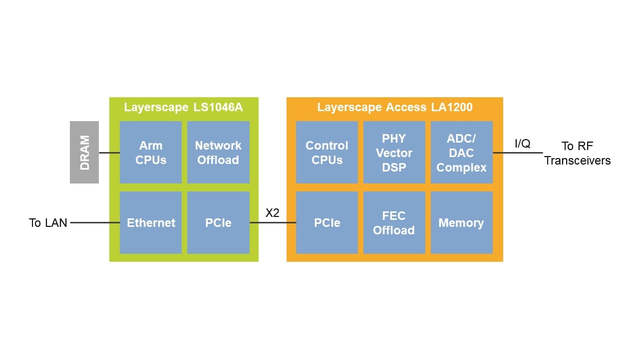
Figure 1: Fixed wireless access (FWA) customer premises equipment (CPE) can use the LS1046A multicore processor for Layer 2 WAN and router functions and the LA12xx processor for 5G Layer 1 functions.
The LA9350 family has about a quarter of the floating-point capability and half the control-processing horsepower as the LA12xx. It’s a small chip, fitting in a 9 x 9 mm BGA package. A 2.5 Gbit/s Ethernet port replaces the PCI interface. It doesn’t include the set of ADC/DAC for mmWave radios. Nonetheless, the LA9350 family serves diverse applications, such as 5G repeaters to light up spaces in the 5G shadows handling digital front-end processing in a 2 x 2 MIMO RU. The lower-cost LA9310 family can sniff 5G airwaves to analyze their quality or extract timing signals and be a digital front end on a single transmit chain. Customers have also shown interest in the LA9300 processors as the backbone in mesh wireless systems, where the backbone can be proprietary and optimized for QoS, resilience and full-duplex performance. Other companies are even using these families in wireline access designs.
Not Just Another Pretty G
The initial products in the LA12xx, LA9350 and LA9310 families will be available in the first quarter of 2020 to members of our early access program. Interested system designers shouldn’t wait to contact their NXP account executives. Development can begin now using the
LA1575 We have an LA1575 reference design board available for use to help develop proofs of concept. More information about NXP’s products for 5G is available at nxp.com/5g.
As it was with our initial Layerscape Access processor, our goal with the new Layerscape Access families is to transform the industry through flexibility. These baseband processors bring openness and intelligence to the physical layer. They’re available to any developer, versatile enough to be used in diverse applications and intelligent because they’re programmable. Redefining the architecture of the RAN and setting the stage for upending the industry, 5G isn’t just another G. Similarly, a Layerscape Access processor isn’t just another chip but instead a software defined platform to implement baseband functions, changing how communication equipment is designed.
Arm is a trademark or registered trademark of Arm Limited (or its subsidiaries) in the US and/or elsewhere. The related technology may be protected by any or all patents, copyrights, designs and trade secrets. All rights reserved.