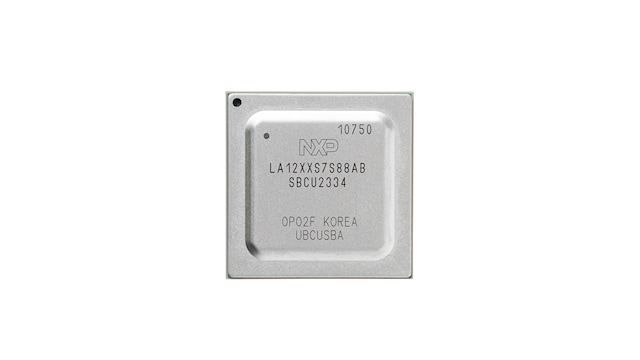
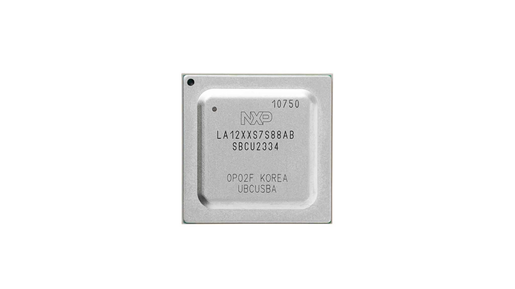
Layerscape® 1046A and 1026A Processors
Contact your sales representative for pricing and buying options.
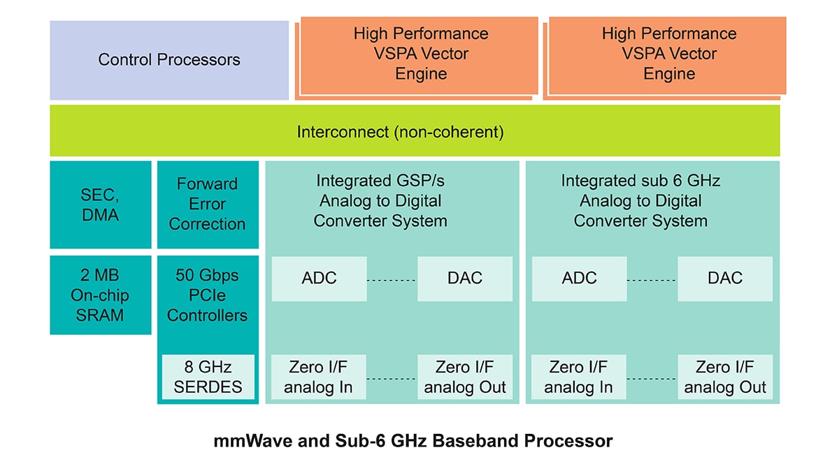
The Layerscape Access LA12xx family of programmable baseband processors delivers high-performance digital signal processing capabilities, performance scalability and application flexibility for 5G sub-6 GHz and mmWave Fixed Wireless Access equipment such as Integrated Small Cells, O-RAN Distributed Unit and Radio Unit and Customer Premises Equipment (CPE). It can be also used in proprietary wireless applications such as defense and civilian radio systems and non-terrestrial networks (NTN).
The family is equipped with a unique combination of:
For additional information and sample availability, contact NXP Support.
| Application | Device Family | Part Number | FECA | DSP-Cores | Low-Speed DCS | High-Speed DCS |
|---|---|---|---|---|---|---|
| O-DU | LA120x | LA1200 | N/A | N/A | ||
| LA1201 | 8x | |||||
| O-RU | LA121x | LA1212 | N/A | 8x | 2T2R | N/A |
| LA1214 | 8x | 4T4R | N/A | |||
| LA1215 | 8x | N/A | mmWave | |||
| LA1216 | 8x | 2T2R | 1*Rx Only | |||
| LA1218 | 8x | 4T4R | 2*Rx Only | |||
| FWA-CPE | LA122x | LA1223 | 8x | 2T2R | N/A | |
| LA1224 | 8x | Dual Use | Dual Use | |||
| LA1325 | 8x | N/A | mmWave | |||
| ISC | LA123x | LA1232 | 8x | 2T2R | N/A | |
| LA1234 | 8x | 4T4R | N/A | |||
| LA1235 | 8x | N/A | mmWave | |||
| LA1236 | 8x | 2T2R | 1*Rx Only | |||
| LA1238 | 8x | 4T4R | 2*Rx Only | |||
Are you working with NXP processors or microcontrollers?
Don’t spend your money solving issues that NXP has already solved.
With NXP’s Premium Support, you’re getting expert help and a contractually obligated agreement for high-quality technical assistance. Enjoy guaranteed response times and direct access to NXP engineers who have likely already solved the issues you are facing.
Benefits include:Click here to discover how Premium Support can optimize your next design.
NXP provides CodeWarrior, the Integrated Development Environment associated with Layerscape Access and many other NXP devices. Included in this environment is a multi-generational, mature compiler as well as access to a rich suite of existing software / signal processing libraries, examples and training material.
A broad ecosystem and comprehensive development platform support is essential to ease development and speed time to market for a commercial grade 3GPP Stacks. All L1 and L2/+ software stack is available from NXP and/or partners depending on the device category and other requirements.
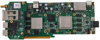
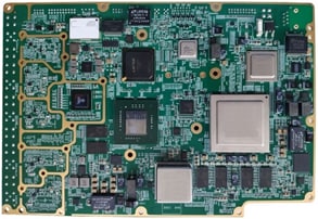
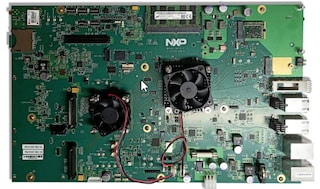
Customers can implement and develop their applications with LA12xx evaluation hardware. The LA12xx Evaluation Board is a combination of NXP LX2160 multicore Arm® processor as host and LA12xx modem as baseband for 5G-NR Fixed Wireless applications. The boards come with pre-loaded board support package (BSP) based on a standard Linux kernel.
|
|
|
|
|
|
|
|---|---|---|---|---|---|
|
|
|
|
|
|
|
|
|
|
|
|
|
|
|
|
|
|
|
|
|
|
|
|
|
|
|
|
|
|
|
|
|
|
|
|
|
|
|
|
|
|
|
|
|
|
|
|
|
|
|
|
|
|
|
|
|
|
|
|
|
|
|
|
|
|
|
|
|
|
Quick reference to our documentation types
1-10 of 22 documents
Compact List
Receive the full breakdown. See the product footprint and more in the eCad file.
2 hardware offerings
Quick reference to our software types.
3 software files
Note: For better experience, software downloads are recommended on desktop.
To get further assistance directly from NXP, please see our Engineering Services.
1-5 of 13 engineering services


To find additional partner offerings that support this product, visit our Partner Marketplace.