
Product Longevity
Participating products are available for a minimum of 10 years. Designated participating products developed for the automotive, telecom and medical segments are available for a minimum of 15 years.
The NX5P3090 is a precision adjustable current-limited power switch for USB PD application. The device includes under voltage lockout, over-temperature protection, and reverse current protection circuits to automatically isolate the switch terminals when a fault condition occurs. The 29V tolerance on VBUS pin ensures the device is able to work on a USB PD port; a current limit input (ILIM) pin defines the over-current limit threshold; an open-drain fault output (FAULT) indicates when a fault condition has occurred.
The over-current limit threshold can be programmed from 400 mA to 3.3 A, using an external resistor between the ILIM pin and GND pin. In the over current condition, the device will clamp the output current to the value set by ILIM and keep the switch on while assert the FAULT flag. To minimize current surges during turn on and turn off, the device has built in soft start which controls the power switch rise and fall time.
Surge protection has been integrated in the device to enhance system robustness. The enable input includes integrated logic level translation making the device compatible with lower voltage processors and controllers.
NX5P3090 is offered in a 12 bump 1.35 × 1.65 mm, 0.4 mm pitch WLCSP package.

Participating products are available for a minimum of 10 years. Designated participating products developed for the automotive, telecom and medical segments are available for a minimum of 15 years.
|
|
|
|
|
|
|
|---|---|---|---|---|---|
|
|
|
|
|
|
|
|
|
|
|
|
|
|
|
|
|
|
|
|
|
|
|
|
|
|
|
|
|
|
|
|
|
|
|
|
|
|
|
|
|
|
|
|
|
|
|
|
|
|
|
|
|
|
|
|
|
|
|
|
|
|
|
|
|
|
|
|
|
|
Quick reference to our documentation types
3 documents
Compact List
Please wait while your secure files are loading.
Receive the full breakdown. See the product footprint and more in the eCad file.

Receive the full breakdown. See the product footprint and more in the eCad file.
1-5 of 8 hardware offerings
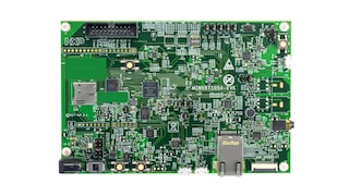
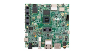
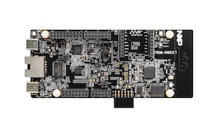
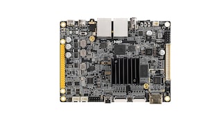
1 engineering service

There are no results for this selection.
To find additional partner offerings that support this product, visit our Partner Marketplace.