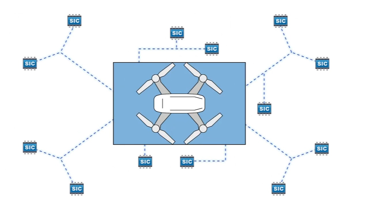
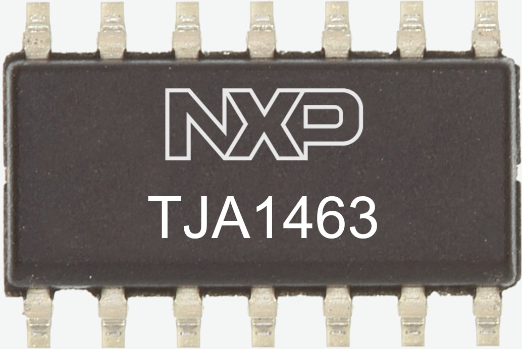
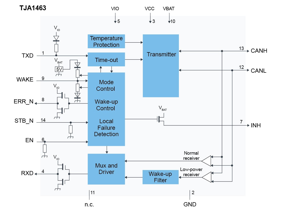
The TJA1463 CAN signal improvement capability (SIC) transceiver with sleep mode is part of the TJA146x transceiver family that implements CAN SIC as defined in CiA 601-4. By meeting the CAN physical layer as defined in ISO11898-2:2016 and SAE J2284-(1-5), the TJA1463 is fully interoperable with high-speed classical CAN and CAN FD.
CAN signal improvement significantly reduces signal ringing on a network, allowing reliable CAN FD communication to function at 5 Mbit/s in larger topologies. In addition, the TJA1462 features a much tighter bit timing symmetry performance to enable CAN FD communication up to 8 Mbit/s.
The TJA1463 is backwards compatible and a drop-in replacement for classical CAN and CAN FD transceivers, such as NXPs TJA1043 and TJA1443.

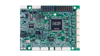
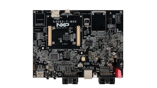
 Complete Solution
 Complete Solution
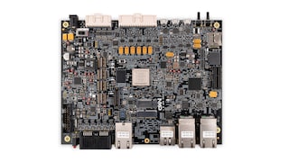 Complete Solution
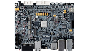 Complete Solution