Product Longevity
Participating products are available for a minimum of 10 years. Designated participating products developed for the automotive, telecom and medical segments are available for a minimum of 15 years.
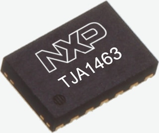
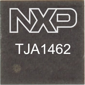
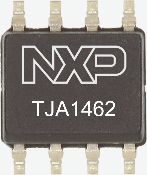
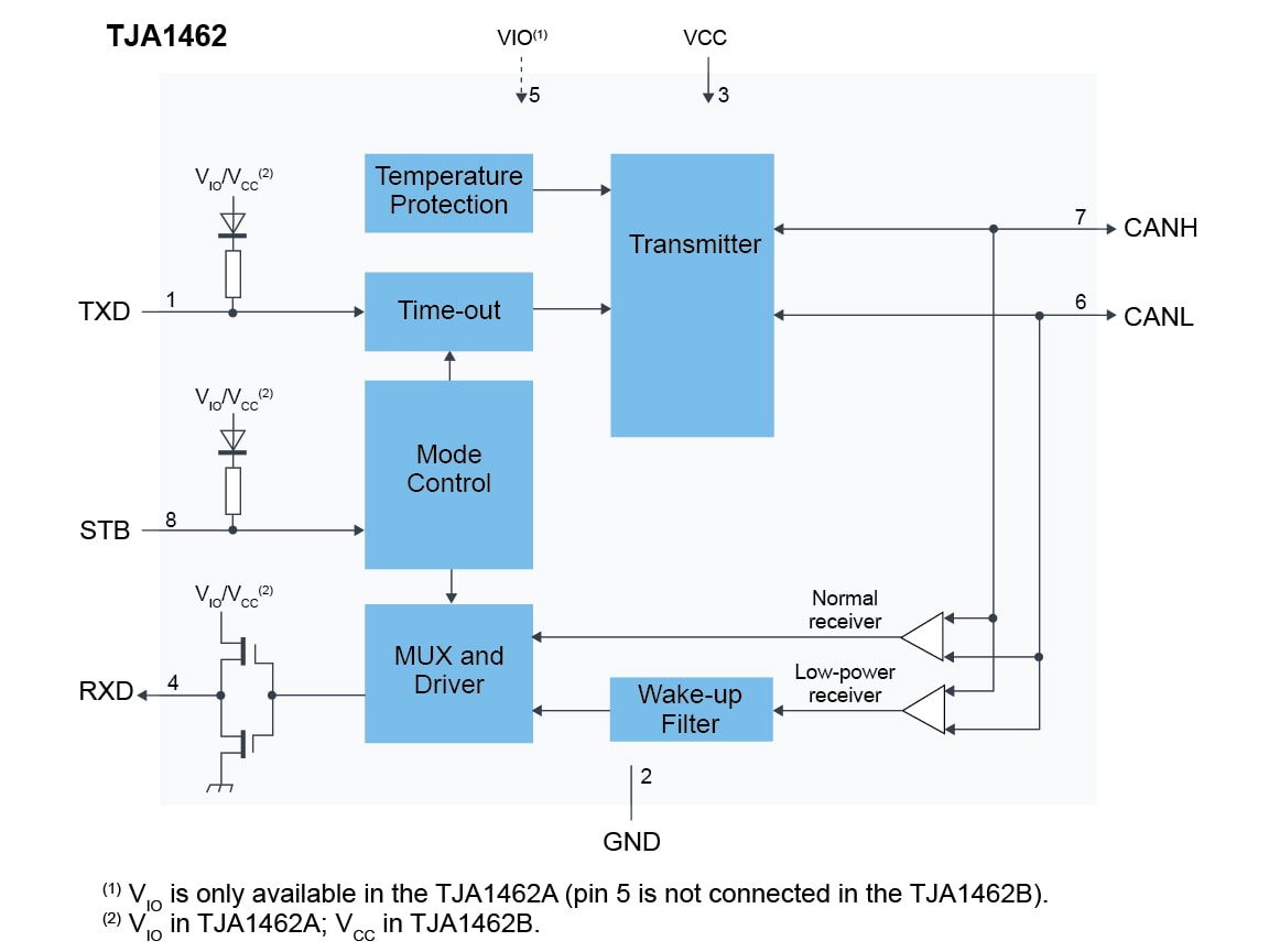
The TJA1462 CAN signal improvement capability (SIC) transceiver with standby mode is part of the TJA146x transceiver family that implements CAN SIC as defined in ISO 11898-2:2024 third edition. By meeting the CAN physical layer as defined in ISO 11898-2:2024 and SAE J2284-(1-5), the TJA1462 is fully interoperable with high-speed classical CAN and CAN FD.
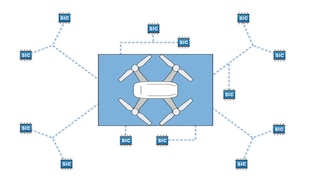
CAN signal improvement significantly reduces signal ringing on a network, allowing reliable CAN FD communication to function at 5 Mbit/s in larger topologies. In addition, the TJA1462 features a much tighter bit timing symmetry performance to enable CAN FD communication up to 8 Mbit/s.
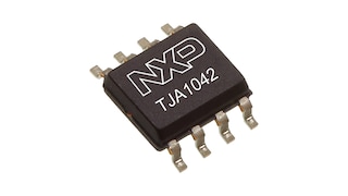
The TJA1462 is backward compatible and a drop-in replacement for classical CAN and CAN FD transceivers, such as NXPs TJA1042 and TJA1044GT.
Participating products are available for a minimum of 10 years. Designated participating products developed for the automotive, telecom and medical segments are available for a minimum of 15 years.
|
|
|
|
|
|
|
|---|---|---|---|---|---|
|
|
|
|
|
|
|
|
|
|
|
|
|
|
|
|
|
|
|
|
|
|
|
|
|
|
|
|
|
|
|
|
|
|
|
|
|
|
|
|
|
|
|
|
|
|
|
|
|
|
|
|
|
|
|
|
|
|
|
|
|
|
|
|
|
|
|
|
|
|
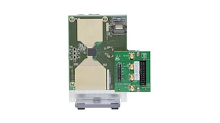
Receive the full breakdown. See the product footprint and more in the eCad file.
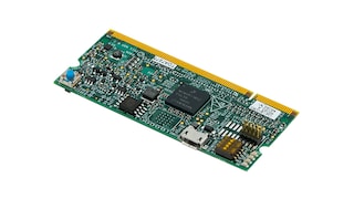
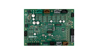
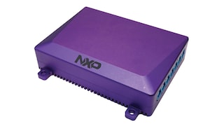
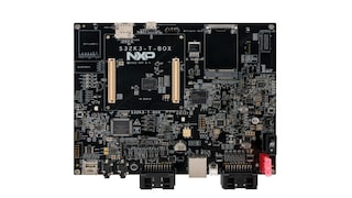
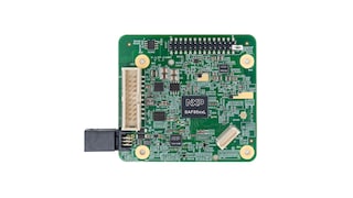
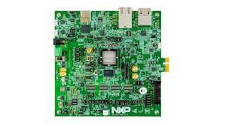
1-5 of 11 hardware offerings

To get further assistance directly from NXP, please see our Engineering Services.
2 engineering services

To find additional partner offerings that support this product, visit our Partner Marketplace.