Hardware
1 hardware offering
-
 Evaluation and Development Boards
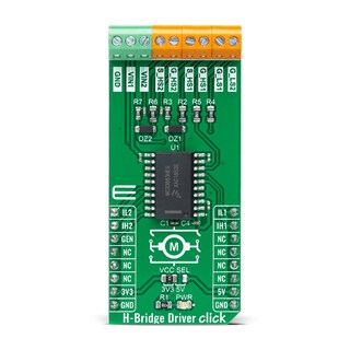
Freedom Platform for MC33883 H-Bridge Gate Driver
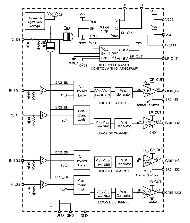
The NXP® MC33883 is an H-bridge gate driver (also known as a full-bridge pre-driver) IC with integrated charge pump and independent high and low side gate driver channels.
Part numbers include: MC33883HEG.
Quick reference to our documentation types.
5 documents
1 hardware offering
To get further assistance directly from NXP, please see our Engineering Services.
1 engineering service

To find a complete list of our partners that support this product, please see our Partner Marketplace.