Quad Integrated Communication Controller (QUICC)

  • Not Recommended for New Designs
  • This page contains information on a product that is not recommended for new designs.

Product Details

Select a section:

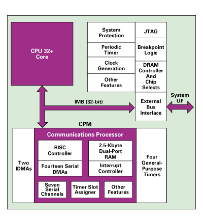
Block Diagram

Quad Integrated Communication Controller Block Diagram

Quad Integrated Communication Controller Block Diagram

Features

  • 32-bit version of the CPU32 core (fully compatible with CPU32)
  • Up to 32-bit Data Bus (Dynamic Bus Sizing for 8- and 16-Bits) + 32 Address Lines
  • Complete static design (0-33 MHz Operation)
  • Follower mode to disable CPU32+ (allows use with external processors)
    • Multiple QUICCs can share one system bus (one leader)
    • MC68040 companion mode allows QUICC to be an MC68040 companion chip and intelligent peripheral (29 MIPS at 33 MHz)
    • All QUICC features available in follower mode
  • Memory controller (eight banks)
    • Contains complete Dynamic Random-Access Memory (DRAM) controller
    • Glueless interface to DRAM Single In-Line Memory Modules (SIMMs), Static Random-Access Memory (SRAM),
    • Electrically Programmable Read-Only Memory (EPROM), Flash EPROM, etc.
    • Boot chip select available at Reset (options for 8-, 16-, or 32-bit memory)
    • Special features for MC68040 including Burst Mode
  • Four general-purpose timers
    • Four 16-bit timers or two 32-bit timers
  • Two Independent DMAs (IDMAs)
  • System Integration Module (SIM60)
    • Bus monitor
    • Breakpoint logic provides on-chip H/W breakpoints
    • Spurious interrupt monitor
    • External leaders may use on-chip features such as chip selects
    • Periodic interrupt timer
    • On-chip bus arbitration with no overhead for internal leaders
    • Low power stop mode
    • IEEE 1149.1 Test Access Port
  • RISC Communications Processor Module (CPM)
    • Many new commands (e.g., Graceful Stop Transmit, Close RxBD)
    • Supports continuos mode transmission and reception on all serial channels
    • 2.5 kbytes of dual-port RAM
    • 14 Serial DMA (SDMA) channels
    • Three parallel I/O registers with open-drain capability
    • Each serial channel can have its own Pins (NMSI mode)
  • Four baud rate generators
  • Four SCCs
    • Ethernet/IEEE 802.3 optional on SCCs 1-2@25 MHz, SCCs 1-3@33 MHz
    • HDLC Bus
    • Universal Asynchronous Receiver Transmitter (UART)
    • Synchronous UART
    • Asynchronous HDLC (RAM microcode option) to support PPP (Point to Point Protocol)
  • Two SMCs
    • UART
    • Transparent
    • General Circuit Interface (GCI) controller
  • One SPI
  • Time-Slot assignor
  • Supports two TDM channels
  • Parallel Interface Port (supports fast connection between QUICCs)

Part numbers include: MC68360AI25L, MC68360AI25VL, MC68360AI33L, MC68360CAI25L, MC68360CRC25L, MC68360CVR25L, MC68360CZQ25L, MC68360VR25L, MC68360VR25VL, MC68360ZQ25VL, MC68360ZQ33L, MC68EN360AI25L, MC68EN360AI25VL, MC68EN360AI33L, MC68EN360CAI25L, MC68EN360CVR25L, MC68EN360CZQ25L, MC68EN360VR25VL, MC68EN360VR33L, MC68EN360ZQ25L, MC68MH360AI25L, MC68MH360VR25VL.

Documentation

Quick reference to our documentation types.

1-5 of 48 documents

Show All

Design Resources

Select a section:

Design Files

2 design files

Software

3 software files

Note: For better experience, software downloads are recommended on desktop.