USB PD and Type-C High-Voltage Sink/Source Combo Switch with Protection
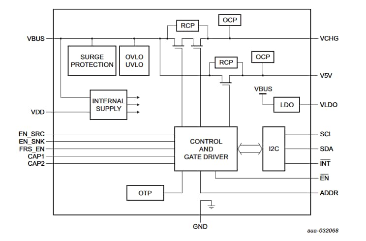
The NX20P3483UK is a product with combined multiple power switches and an LDO for USB PD application. The device includes a bi-directional high-voltage power switch which supports both 20V sink and 6V source; a 5V power switch for source and a 100mA LDO provides a power supply for dead battery operation.
The high-voltage power switch has 29V DC tolerance and is able to sink up to 5A at a maximum of 20V and source up to 3.4A at a maximum of 6V. When it is configured as a high-voltage sink switch, the path has overvoltage protection and reverse current protection features. While it is configured as a high-voltage source switch, the adjustable overcurrent limit circuit is integrated.
Product Details
Features
Key Features
- Wide supply voltage range for VBUS from 2.8V to 20V
- System power supply V5V from 4.0V to 5.5V
- Chip power supply VDD from 2.7V to 5.5V
- VBUS to VCHG Bi-directional Switch
- V5V to VBUS Switch
- Integrated high-voltage LDO with reverse voltage protection
- Supports four different I2C target addresses by ADDR pin
- ESD protection
- Safety Approvals for UL and CB
- OVP, OCP, SCP and RCP Protections for the switches
- IEC61000-4-5 Surge protection up to 95V
Product Longevity Program
- This product is included in the NXP Product Longevity Program ensuring a stable supply of products for your embedded designs. The NX20P3483UK is included in the 10-year program
Part numbers include: NX20P3483UK.
Design Resources
Engineering Services
To get further assistance directly from NXP, please see our Engineering Services.
1 engineering service
-
Independent Design House (IDH)
Embedded Software Design

To find additional partner offerings that support this product, visit our Partner Marketplace.