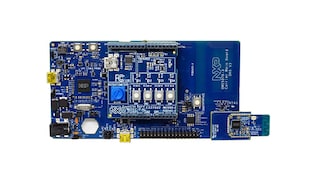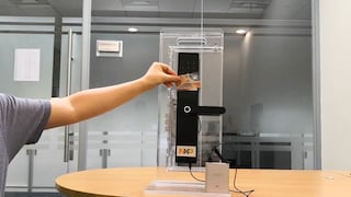


Fully Certified Module Supporting Bluetooth and NFC
Design Files
Quick reference to our
design files types.
2 design files
Receive the full breakdown. See the product footprint and more in the eCad file.
-
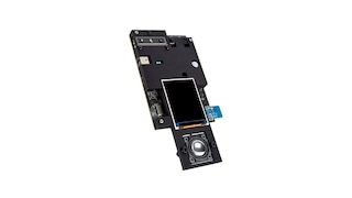
Printed Circuit Boards and Schematics
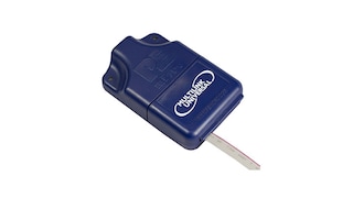
Coin Cell Hardware Design Files.
-
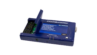
Printed Circuit Boards and Schematics
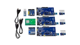
QN9090 Design Kit Hardware Design Files