MPC8533E PowerQUICC® III Processor

  • MPC8533 device is "Not recommended for new designs", please use the\n replacement families Power Architecture (T1013,\n T1023),\n Arm Architecture (LS1012A, LS1023A).

Block Diagram

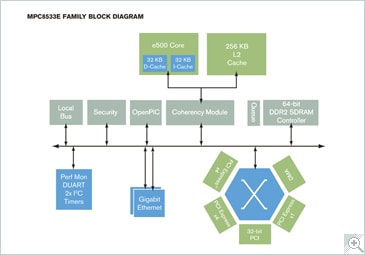
MPC8533E Block Diagram

Features

  • Embedded e500 core, initial offerings up to 667 MHz, targeting up to 1.0 GHz
    • Dual dispatch superscalar, 7-stage pipeline design with out-of-order issue and execution
    • 2,240 MIPS at 1.0 GHz (estimated Dhrystone 2.1)
    • 36-bit physical addressing
  • Enhanced hardware and software debug support
  • Double-precision embedded scalar and vector floating-point APUs
  • Memory management unit (MMU)
  • Double-precision embedded scalar and vector floating-point APUs
  • Integrated L1/L2 cache
    • L1 cache—32 KB data and 32 KB instruction cache with line-locking support
    • L2 cache—256 KB (8-way set associative); 256/128/64/32 KB can be used as SRAM
    • L1 and L2 hardware coherency
    • L2 cache and I/O transactions can be stashed into L2 cache regions
  • Integrated DDR memory controller with full ECC support, offering:
    • 200 MHz clock rate (400 MHz data rate), 64-bit, 2.5V/2.6V I/O, DDR SDRAM
    • 267 MHz clock rate (up to 533 MHz data rate), 64-bit, 1.8V I/O, DDR2 SDRAM
  • Integrated security engine supporting DES, 3DES, MD-5, SHA-1/2, AES, RSA, RNG, Kasumi F8/F9 and ARC-4 encryption algorithms
  • Two on-chip Three Speed Ethernet controllers (ETSECs) supporting 10 Mbps, 100 Mbps and 1 Gbps Ethernet/IEEE® 802.3 networks with MII, RMII, RGMII, and RTBI physical interfaces:
    • TCP/UDP/IP checksum acceleration
    • Advanced QoS features
  • General-purpose input/output (GPIO)
  • PCI Express high-speed interconnect interfaces, supporting combinations of dual x4 and single x1 PCI Express
  • On-chip network (OCeaN) switch fabric
  • PCI interface support
    • 32-bit PCI 2.2 bus controller (up to 66MHz, 3.3V I/O)
  • Local bus
    •  166 MHz, 32-bit, 3.3V I/O, local bus with memory controller
  • Integrated four-channel DMA controller
    •  Multiplexed 32-bit address and data operating up to 133 MHz
    •  32-, 16- and 8-bit port sizes controlled by on-chip memory controller
  • Dual I²C and DUART support
  • Dual I²C interfaces (controller or target mode)
  • Programmable interrupt controller (PIC)
  • IEEE 1149.1 JTAG test access port
  • 1.0V core voltage with 3.3V and 2.5V I/O
  • 783-pin FC-BGA package
  • Buy/Parametrics


    Documentation

    Quick reference to our documentation types.

    1-5 of 49 documents

    Show All

    Design Files

    Quick reference to our design files types.

    1 design file

    Hardware

    Quick reference to our board types.

    2 hardware offerings

    Software

    Quick reference to our software types.

    3 software files

    Note: For better experience, software downloads are recommended on desktop.

    Engineering Services

    1-5 of 6 engineering services

    Show All

    To find additional partner offerings that support this product, visit our Partner Marketplace.

    Training

    7 trainings

    Show All

    Support

    What do you need help with?