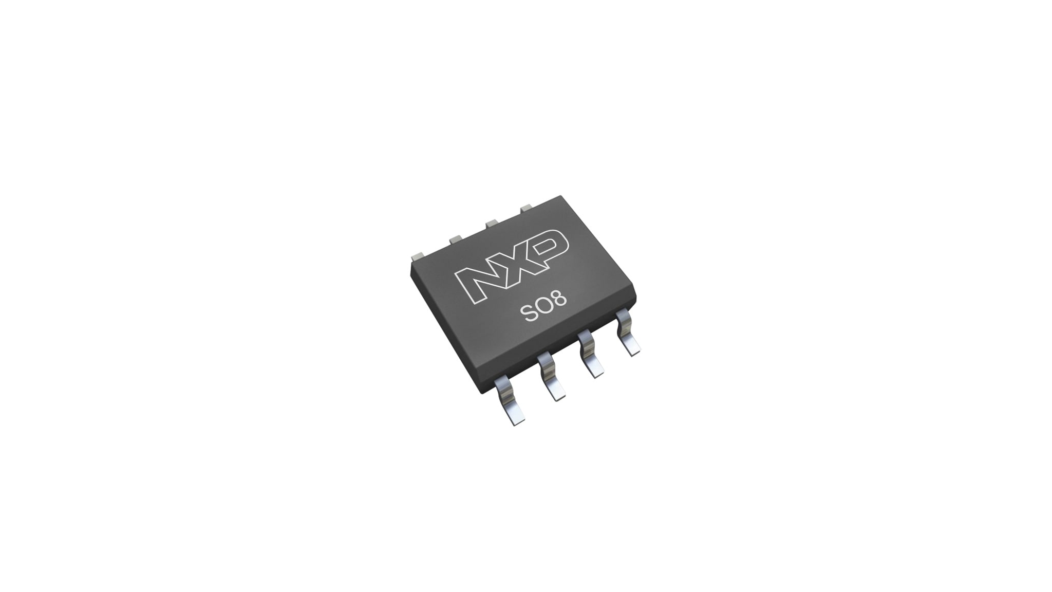
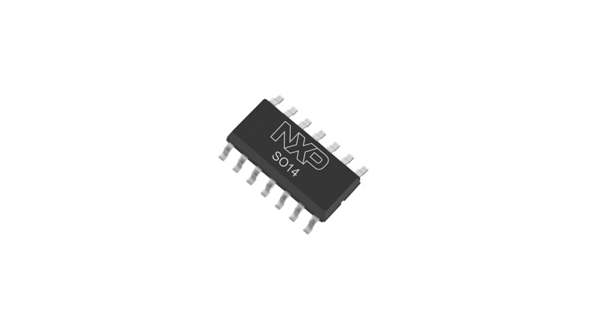
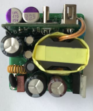
Synchronous Rectification Controller with Integrated Feedback and Protection

Roll over image to zoom in

Block Diagram

TEA1761T / TEA1762T

TEA1761T Block Diagram

Features

Key Features

  • Combined synchronous rectification and primary feedback control functionality
  • Wide supply voltage range (8.6 V to 38 V)
  • High level of integration, resulting in a very low external component count
  • Wide opto coupler output voltage range (3.5 V to 38 V)
  • Accurate internal voltage reference for voltage control (within 1 %)
  • Separate sense ground for accurate voltage sensing
  • High driver output voltage of 10 V to drive all MOSFET brands to the lowest RDSon
  • Reference voltage output pin
  • Low current consumption
  • High system efficiency from no load to full load
  • Undervoltage protection
  • General purpose protection input pin
  • Internal over-temperature protection

NXP GreenChip

  • This product is part of the NXP GreenChip portfolio, this program optimizes for energy efficiency in mobile and computing applications, specializing in high-power density, safety and reliability.

Buy/Parametrics


Documentation

Quick reference to our documentation types.

1-5 of 9 documents

Show All

Design Files

Hardware

Quick reference to our board types.

2 hardware offerings

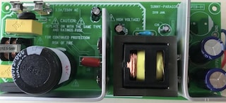
  • 165W Battery Charger
    Complementary Silicon or Component

    165W Battery Charger

  • 30W Dual Port PD Charger
    Complementary Silicon or Component

    30W Dual Port PD Charger

Support

What do you need help with?