Hardware
1 hardware offering
-
 Evaluation and Development Boards
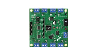
Evaluation Kit MC33882 -Smart Six Output Switch with SPI and Parallel Input ControlFeatured
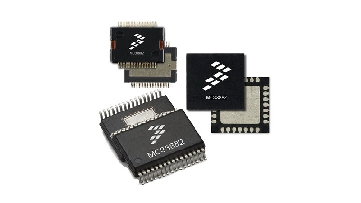
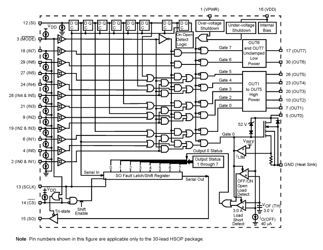
The NXP® MC33882 is a six-output, low side switch that controls system loads up to 1.0 A. The six outputs can be controlled via both serial peripheral interface (SPI) and parallel input control, ideal for fault tolerant system applications.
Part numbers include: MC33882PEK, MC33882PEP, MC33882PVW.
Quick reference to our documentation types.
4 documents
1 hardware offering
To get further assistance directly from NXP, please see our Engineering Services.
3 engineering services


To find a complete list of our partners that support this product, please see our Partner Marketplace.