Please check the new test online
NFC Antenna Tool
for tag and reader devices.
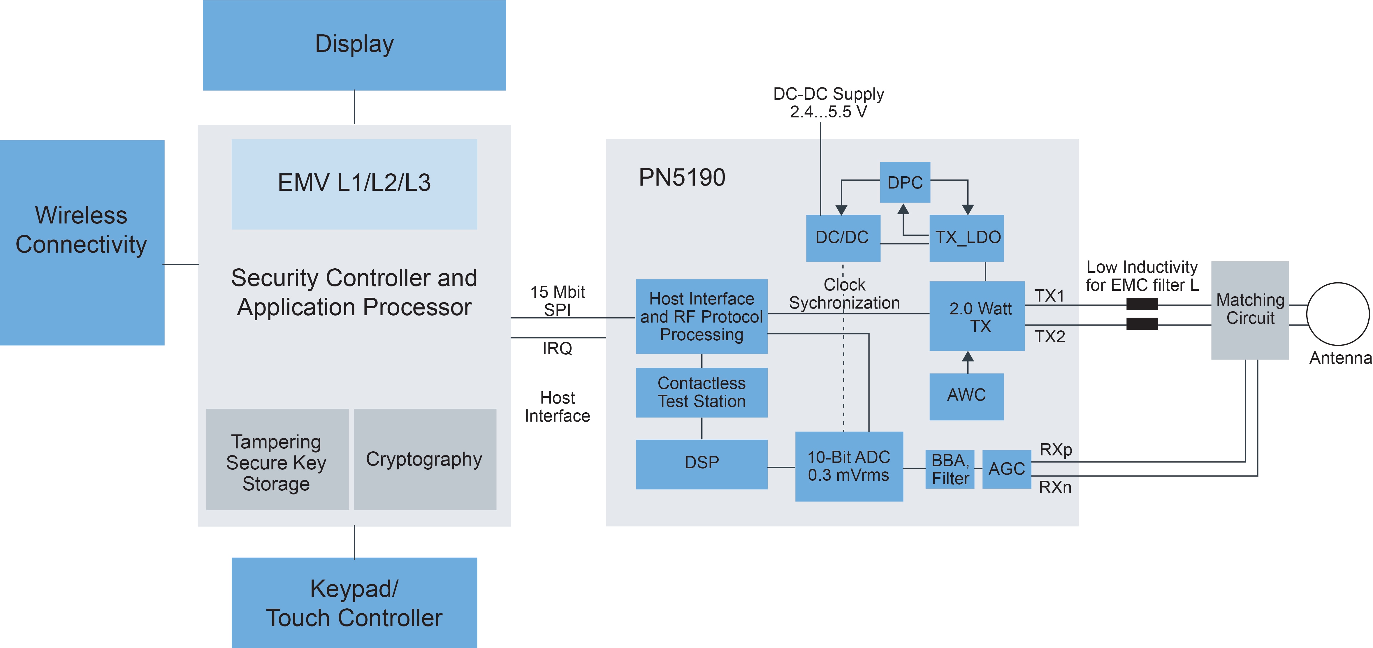
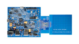
As a full NFC frontend with High RF output (2.0W) and High receiver sensitivity, the NXP PN5190 is a robust solution for payment terminals and all readers that need to generate a strong RF field in a difficult environment.
The PN5190 simplifies design while ensuring interoperability with a broad range of smartcards and mobile phones and allows to achieve EMVCo 3.2 analog and digital L1 compliancy.
The High output power and receiver sensitivity allow the design of small antennas. Efficient power-saving modes allow a long battery lifetime for battery-powered systems, including residential access locks.
A fast antenna design is supported by the NFC Antenna Design Hub, the PC based configuration tool "NFC Cockpit" enables simple configuration (e.g. RF register settings, DPC, AWC ) and EMVCo compliance testing of a design. The Feature complete software support - the NFC reader Library - gives developers a faster and simpler way to develop NFC-enabled products.
