Design Files
2 design files
Receive the full breakdown. See the product footprint and more in the eCad file.
-
Models
IBIS models for LPC29xx
-
Symbols and Footprints
LPC2xxx ORCAD symbols
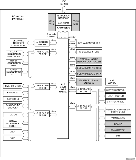
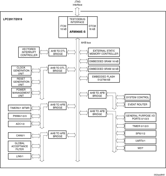
The LPC2917/2919/01 combine an ARM968E-S CPU core with two integrated TCM blocks operating at frequencies of up to 125 MHz, CAN and LIN, 56 kB SRAM, up to 768 kB flash memory, external memory interface, two 10-bit ADCs, and multiple serial and parallel interfaces in a single chip targeted at consumer, industrial, medical, and communication markets. To optimize system power consumption, the LPC2917/2919/01 has a very flexible Clock Generation Unit (CGU) that provides dynamic clock gating and scaling.
Choose a diagram:
Note: To see the product features close this window.
|
|
|
|
|
|
---|---|---|---|---|---|
|
|
|
|
|
|
|
|
|
|
|
|
|
|
|
|
|
|
|
|
|
|
|
|
|
|
|
|
|
|
|
|
|
|
|
|
|
|
|
|
|
|
|
|
|
|
|
|
|
|
|
|
|
|
|
|
|
|
|
|
Quick reference to our documentation types.
1-5 of 16 documents
Please wait while your secure files are loading.
2 design files
Receive the full breakdown. See the product footprint and more in the eCad file.
Please wait while your secure files are loading.