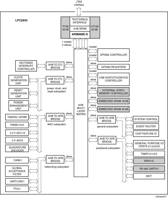
Arm9 flashless microcontroller with CAN, LIN, and USB

LPC2930FBD208
  • Not Recommended for New Designs
  • This page contains information on a product that is not recommended for new designs.

See product image

Product Details

Select a section:

Block Diagram

Block diagram: LPC2930FBD208

Features

Main Features

  • ARM968E-S processor running at frequencies of up to 125 MHz maximum.
  • Multi-layer AHB system bus at 125 MHz with three separate layers.
  • Dual-leader, eight-channel GPDMA controller on the AHB multilayer matrix which can be used with the SPI interfaces and the UARTs, as well as for memory-to-memory transfers including the TCM memories.
  • External Static Memory Controller (SMC) with eight memory banks; up to 32-bit data bus; up to 24-bit address bus.
  • Up to 152 general-purpose I/O pins with programmable pull-up, pull-down, or bus keeper.
  • Vectored Interrupt Controller (VIC) with 16 priority levels.
  • Up to 22 level-sensitive external interrupt pins, including USB, CAN and LIN wake-up features.
  • Configurable clock-out pin for driving external system clocks.
  • Processor wake-up from power-down via external interrupt pins; CAN or LIN activity.
  • Flexible Reset Generator Unit (RGU) able to control resets of individual modules.
  • Second CGU (CGU1) with its own PLL generates a configurable clock output.
  • Processor wake-up from power-down via external interrupt pins, CAN, or LIN activity.
  • Standard Arm® test and debug interface with real-time in-circuit emulator.
  • Boundary-scan test supported.
  • ETM/ETB debug functions with 8 kB of dedicated SRAM also accessible for application code and data storage.
  • 144-pin LQFP package.
  • -40 °C to +85 °C ambient operating temperature range.

On-chip memory

  • Two Tightly Coupled Memories (TCM), 32 kB Instruction TCM (ITCM), 32 kB Data TCM (DTCM).
  • Two separate internal Static RAM (SRAM) instances; 32 kB SRAM and 16 kB SRAM.
  • 8 kB ETB SRAM also usable for code execution and data.

Serial interfaces

  • USB 2.0 full-speed Host/OTG/Device controller with dedicated DMA controller and on-chip device PHY.
  • Two-channel CAN controller supporting FullCAN and extensive message filtering
  • Two LIN leader controllers with full hardware support for LIN communication. The LIN interface can be configured as UART to provide two additional UART interfaces.
  • Two 550 UARTs with 16-byte Tx and Rx FIFO depths, DMA support, modem control, and RS-485/EIA-485 (9-bit) support.
  • Three full-duplex Q-SPIs with four follower-select lines; 16 bits wide; 8 locations deep; Tx FIFO and Rx FIFO.
  • Two I²C-bus interfaces.

Flexible Clock-Generation Unit (CGU0) able to control clock frequency of individual modules

  • On-chip very low-power ring oscillator; fixed frequency of 0.4 MHz; always on to provide a Safe_Clock source for system monitoring.
  • On-chip crystal oscillator with a recommended operating range from 10 MHz to 25 MHz. PLL input range 10 MHz to 25 MHz.
  • On-chip PLL allows CPU operation up to a maximum CPU rate of 125 MHz.
  • Generation of up to 11 base clocks.
  • Seven fractional dividers.

Highly configurable system Power Management Unit (PMU)

  • clock control of individual modules.
  • allows minimization of system operating power consumption in any configuration.

Dual power supply

  • CPU operating voltage: 1.8 V ± 5 %.
  • I/O operating voltage: 2.7 V to 3.6 V; inputs tolerant up to 5.5 V.

Other peripherals

  • One 10-bit ADC with 5.0 V measurement range and eight input channels with conversion times as low as 2.44 μs per channel.
  • Two 10-bit ADCs, 8-channels each, with 3.3 V measurement range provide an additional 16 analog inputs with conversion times as low as 2.44 μs per channel. Each channel provides a compare function to minimize interrupts.
  • Multiple trigger-start option for all ADCs: timer, PWM, other ADC, and external signal input.
  • Four 32-bit timers each containing four capture-and-compare registers linked to I/Os.
  • Four six-channel PWMs (Pulse-Width Modulators) with capture and trap functionality.
  • Two dedicated 32-bit timers to schedule and synchronize PWM and ADC.
  • Quadrature encoder interface that can monitor one external quadrature encoder.
  • 32-bit watchdog with timer change protection, running on safe clock.

Part numbers include: LPC2930FBD208.

Documentation

Quick reference to our documentation types.

1-5 of 13 documents

Show All

Design Resources

Select a section:

Design Files

2 design files

Support

What do you need help with?