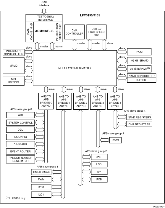
Low-cost, low-power Arm926EJ-S MCUs with high-speed USB 2.0 OTG, SD/MMC, and NAND flash controller

  • This page contains information on a product that is not recommended for new designs.

See product image

Product Details

Block Diagram

Block diagram: LPC3130FET180, LPC3131FET180

Features

CPU platform

  • 180 MHz, 32-bit ARM926EJ-S
  • 16 kB D-cache and 16 kB I-cache
  • Memory Management Unit (MMU)

Internal memory

  • 96 kB (LPC3130) or 192 kB (LPC3131) embedded SRAM

External memory interface

  • NAND flash controller with 8-bit ECC
  • 8/16-bit Multi-Port Memory Controller (MPMC): SDRAM and SRAM

Communication and connectivity

  • High-speed USB 2.0 (OTG, Host, Device) with on-chip PHY
  • Two I²S-bus interfaces
  • Integrated leader/follower SPI
  • Two controller/target I²C-bus interfaces
  • Fast UART
  • Memory Card Interface (MCI): MMC/SD/SDIO/CE-ATA
  • Four-channel 10-bit ADC
  • Integrated 4/8/16-bit 6800/8080 compatible LCD interface

System functions

  • Dynamic clock gating and scaling
  • Multiple power domains
  • Selectable boot-up: SPI flash, NAND flash, SD/MMC cards, UART, or USB
  • DMA controller
  • Four 32-bit timers
  • Watchdog timer
  • PWM module
  • Random Number Generator (RNG)
  • General Purpose I/O (GPIO) pins
  • Flexible and versatile interrupt structure
  • JTAG interface with boundary scan and Arm® debug access

Operating voltage and temperature

  • Core voltage: 1.2 V
  • I/O voltage: 1.8 V, 2.8 V, 3.3 V
  • Temperature: -40 Cel to +85 Cel
  • TFBGA180 package: 12 x 12 mm², 0.8 mm pitch

Buy/Parametrics


Documentation

Quick reference to our documentation types.

1-10 of 11 documents

Compact List

Application Note (6)
Brochure (1)
Data Sheet (1)
Package Information (1)
Supporting Information (1)
User Guide (1)

Design Resources

Design Files

Quick reference to our design files types.

2 design files

Support

What do you need help with?