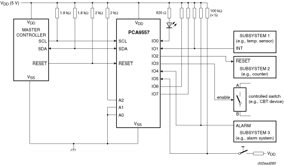
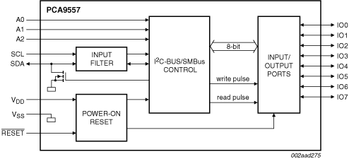
The PCA9557 is a silicon CMOS circuit which provides parallel input/output expansion for SMBus and I²C-bus applications. The PCA9557 consists of an 8-bit input port register, 8-bit output port register, and an I²C-bus/SMBus interface. It has low current consumption and a high-impedance open-drain output pin, IO0.
The system controller can enable the PCA9557's I/O as either input or output by writing to the configuration register. The system controller can also invert the PCA9557 inputs by writing to the active HIGH polarity inversion register. Finally, the system controller can reset the PCA9557 in the event of a time-out by asserting a LOW in the reset input.
The power-on reset puts the registers in their default state and initializes the I²C-bus/SMBus state machine. The RESET pin causes the same reset/initialization to occur without de-powering the part.