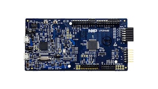
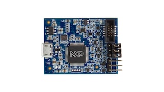
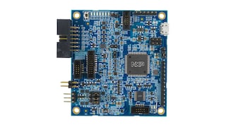
Low-Power Microcontrollers (MCUs) Based on Arm® Cortex®-M4 Cores With Optional Cortex®-M0+ Co-processor

製品詳細

セクションを選択:

ブロック図

LPC541xx MCU

LPC541xx MCU Family Block Diagram

Features

Arm Cortex-M4 core (version r0p1)

  • Arm Cortex-M4 processor, running at a frequency of up to 150 MHz.
  • Floating Point Unit (FPU) and Memory Protection Unit (MPU).
  • Arm Cortex-M4 built-in Nested Vectored Interrupt Controller (NVIC).
  • Non-maskable Interrupt (NMI) input with a selection of sources.
  • Serial Wire Debug (SWD) with six instruction break points, two literal comparators, and four watchpoints. Includes Serial Wire Output for enhanced debug capabilities.
  • System tick timer.

Arm Cortex-M0+ core

  • Arm Cortex-M0+ processor, running at a frequency of up to 150 MHz (uses the same clock as Cortex-M4) with a single-cycle multiplier and a fast single-cycle I/O port.
  • Arm Cortex-M0+ built-in Nested Vectored Interrupt Controller (NVIC).
  • Non-maskable Interrupt (NMI) input with a selection of sources.
  • Serial Wire Debug with four breakpoints and two watchpoints.
  • System tick timer.

On-chip memory

  • Up to 256 KB on-chip flash program memory with the flash accelerator and 256-byte page erase and write.
  • Up to 192 KB total SRAM consisting of 160 KB contiguous main SRAM and an additional 32 KB SRAM on the I&D buses.

ROM API supports

  • Flash In-Application Programming (IAP) and In-System Programming (ISP).
  • ROM-based USB drivers (HID, CDC, MSC, and DFU). Flash updates via USB is supported.
  • Supports booting from valid user code in flash, USART, SPI, and I2C.
  • Legacy, Single, and Dual image boot.

Serial interfaces

  • Flexcomm Interface contains eight serial peripherals. Each can be selected by software to be a USART, SPI, or I2C interface. Two Flexcomm Interfaces also include an I2S interface. Each Flexcomm Interface includes a FIFO that supports USART, SPI, and I2S if supported by that Flexcomm Interface. A variety of clocking options are available to each Flexcomm Interface and include a shared fractional baud-rate generator.
  • I2C-bus interfaces support Fast-mode and Fast-mode Plus with data rates of up to 1Mbit/s and with multiple address recognition and monitor mode. Two sets of true I2C pads also support high-speed mode (3.4 Mbit/s) as a target.
  • Crystal-less USB full-speed device interface.

Digital peripherals

  • DMA controller with 20 channels and 20 programmable triggers, able to access all memories and DMA-capable peripherals.
  • Up to 48 General-Purpose Input/Output (GPIO) pins. Most GPIOs have configurable pull-up/pull-down resistors, programmable open-drain mode, and input inverter.
  • GPIO registers are located on the AHB for fast access.
  • Up to eight GPIOs can be selected as pin interrupts (PINT), triggered by rising, falling or both input edges.
  • Two GPIO grouped interrupts (GINT) enable an interrupt based on a logical (AND/OR) combination of input states.
  • CRC engine.

Analog peripherals

  • 12-bit ADC with 12 input channels and with multiple internal and external trigger inputs and sample rates of up to 5.0 MSamples/sec. The ADC supports two independent conversion sequences.
  • Integrated temperature sensor connected to the ADC.

Timers

  • Five 32-bit standard general purpose timers/counters, four of which support up to four capture inputs and four compare outputs, PWM mode, and external count input. Specific timer events can be selected to generate DMA requests. The fifth timer does not have external pin connections and may be used for internal timing operations.
  • One SCTimer/PWM with eight input and eight output functions (including capture and match). Inputs and outputs can be routed to or from external pins and internally to or from selected peripherals. Internally, the SCTimer/PWM supports ten captures/matches, ten events, and ten states.
  • 32-bit Real-time clock (RTC) with 1 s resolution running in the always-on power domain. A timer in the RTC can be used for wake-up from all low power modes including deep power-down, with 1 ms resolution.
  • Multiple-channel multi-rate 24-bit timer (MRT) for repetitive interrupt generation at up to four programmable, fixed rates.
  • Windowed Watchdog Timer (WWDT).

Clock generation

  • 12 MHz internal Free Running Oscillator (FRO). This oscillator provides a selectable 48 MHz or 96 MHz output, and a 12 MHz output (divided down from the selected higher frequency) that can be used as a system clock. The FRO is trimmed to ±1 % accuracy over the entire voltage and temperature range.
  • External clock input for clock frequencies of up to 25 MHz.
  • Watchdog oscillator (WDTOSC) with a frequency range of 6 kHz to 1.5 MHz.
  • 32.768 kHz low-power RTC oscillator.
  • System PLL allows CPU operation up to the maximum CPU rate without the need for a high-frequency external clock. Can be run from the internal FRO 12 MHz output, the external clock input CLKIN, or the RTC oscillator.
  • Clock output function with divider.
  • Frequency measurement unit for measuring the frequency of on-chip or off-chip clock signal.

Power control

  • Programmable PMU (Power Management Unit) to minimize power consumption and to match requirements at different performance levels.
  • Reduced power modes: sleep, deep-sleep, and deep power-down.
  • Wake-up from deep-sleep modes due to activity on the USART, SPI, and I2C peripherals when operating as followers
  • The Micro-Tick Timer running from the watchdog oscillator can be used to wake-up the device from any reduced power modes.
  • Power-On Reset (POR).
  • Brown-Out-Detect (BOD) with separate thresholds for interrupt and forced the reset.

Additional information

  • Dual processor cores: Arm Cortex-M4 and Arm Cortex-M0+. Both cores operate up to a maximum frequency of 150 MHz.
  • DMIC subsystem including a dual-channel PDM microphone interface, flexible decimators, 16 entry FIFOs, optional DC locking, hardware voice activity detection, and the option to stream the processed output data to I2S.
  • Single power supply 1.62 V to 3.6 V.
  • JTAG boundary scan supported.
  • 128-bit unique device serial number for identification.
  • Operating temperature range -40 °C to +105 °C.
  • Available as WLCSP49 and LQFP64 packages.
  • Supported by MCUXpresso SDK, IDE and Config Tools

部品番号: LPC54101J256BD64, LPC54101J256UK49, LPC54101J512BD64, LPC54101J512UK49, LPC54102J256BD64, LPC54102J256UK49, LPC54102J512BD64, LPC54102J512UK49, LPC54113J256BD64, LPC54113J256UK49, LPC54114J256BD64, LPC54114J256UK49.

ドキュメンテーション

クイック・リファレンス ドキュメンテーションの種類.

1-5 の 37 ドキュメント

全て表示

設計・ファイル

1-5 の 9 設計・ファイル

全て表示

ハードウェア

1-5 の 7 ハードウェア提供

全て表示

ソフトウェア

1-5 の 9 ソフトウェア・ファイル

全て表示

注: より快適にご利用いただくために、ソフトウェアのダウンロードはデスクトップで行うことを推奨します。

エンジニアリング・サービス

1-5 の 17 エンジニアリング・サービス

全て表示

本製品をサポートするパートナーの一覧は、 パートナーマーケットプレイス.

トレーニング

1 トレーニング

サポート

お困りのことは何ですか??