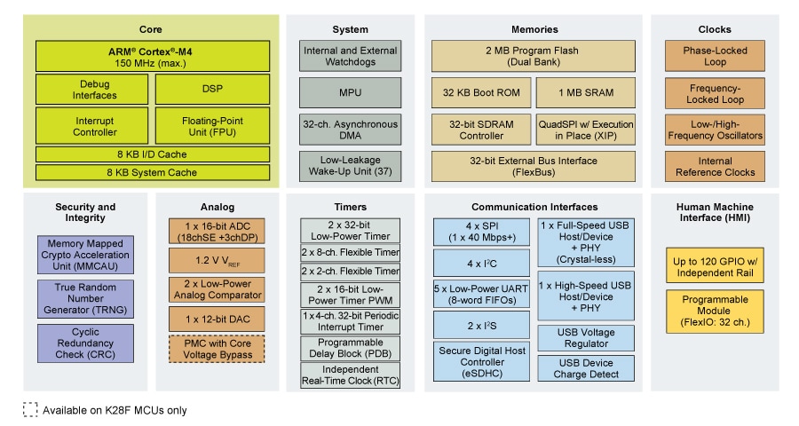
The Kinetis K28 USB Arm® Cortex®-M4 MCUs target applications requiring processing efficiency and extra-large embedded memory with 2 MB Flash and 1 MB SRAM. This microcontroller sub-family is:
- Highly integrated with two I2S interfaces, two USB Controllers (High-Speed with integrated High-Speed PHY and Full-Speed) and mainstream analog peripherals
- Expandable through a 32-bit SDRAM memory controller and QuadSPI interface supporting eXecution-In-Place (XiP)
- Enabling secure content using a True Random Number Generator, Cyclic Redundancy Check, Memory Mapped Cryptographic Acceleration Unit
3 Input supply voltage rails: (1.2V, 1.8V and 3V) + separate VBAT domain
K28 implements a Power Management Controller supporting Core Voltage Bypass and can be powered by an external PMIC to maximize the power efficiency of the overall system
Packages: 169 MAPBGA (9 x 9 mm², 0.65mm pitch) and 210 WLCSP (6.9 x 6.9 mm², 0.4 mm pitch)
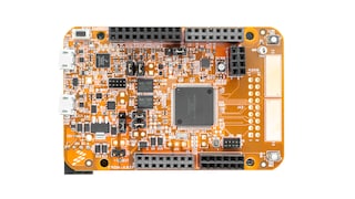
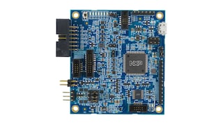
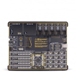
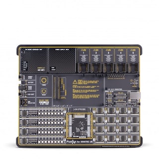
Evaluation / Development platform: FRDM-K28F