Product Longevity
Participating products are available for a minimum of 10 years. Designated participating products developed for the automotive, telecom and medical segments are available for a minimum of 15 years.
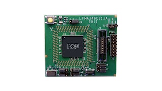
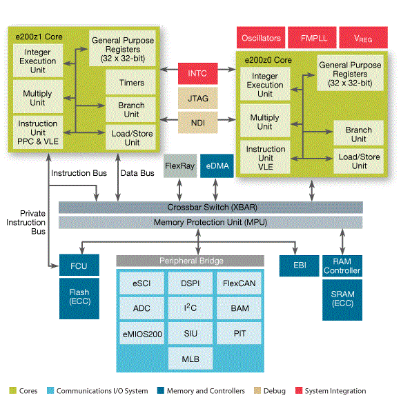
Designed for body electronics, the NXP MPC5510 MCU belongs to an expanding family of automotive-focused products that address the next wave of central body and gateway applications within the vehicle.
Participating products are available for a minimum of 10 years. Designated participating products developed for the automotive, telecom and medical segments are available for a minimum of 15 years.
|
|
|
|
|
|
|
|---|---|---|---|---|---|
|
|
|
|
|
|
|
|
|
|
|
|
|
|
|
|
|
|
|
|
|
|
|
|
|
|
|
|
|
|
|
|
|
|
|
|
|
|
|
|
|
|
|
|
|
|
|
|
|
|
|
|
|
|
|
|
|
|
|
|
|
|
|
|
|
|
|
|
|
|
Quick reference to our documentation types
1-10 of 52 documents
Compact List
2 design files
Receive the full breakdown. See the product footprint and more in the eCad file.
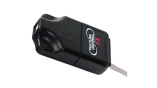
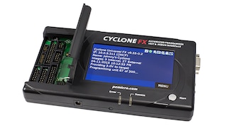
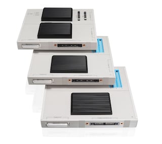
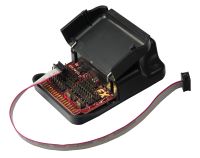
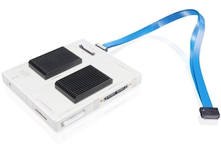
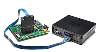
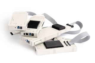
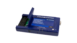
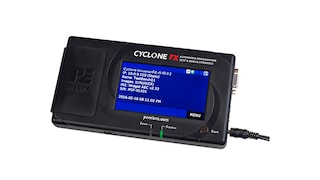
1-5 of 7 hardware offerings
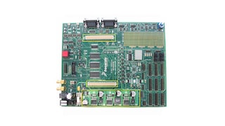
Additional hardware available. View our featured partner solutions.
Quick reference to our software types.
4 software files
Additional software available. View our featured partner solutions.
Note: For better experience, software downloads are recommended on desktop.
To get further assistance directly from NXP, please see our Engineering Services.
1-5 of 13 engineering services


To find additional partner offerings that support this product, visit our Partner Marketplace.
5 trainings