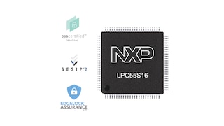
LPC550x/S0x: Baseline Arm® Cortex®-M33-Based Microcontroller Family
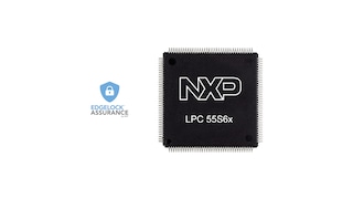
Click image to open expanded view

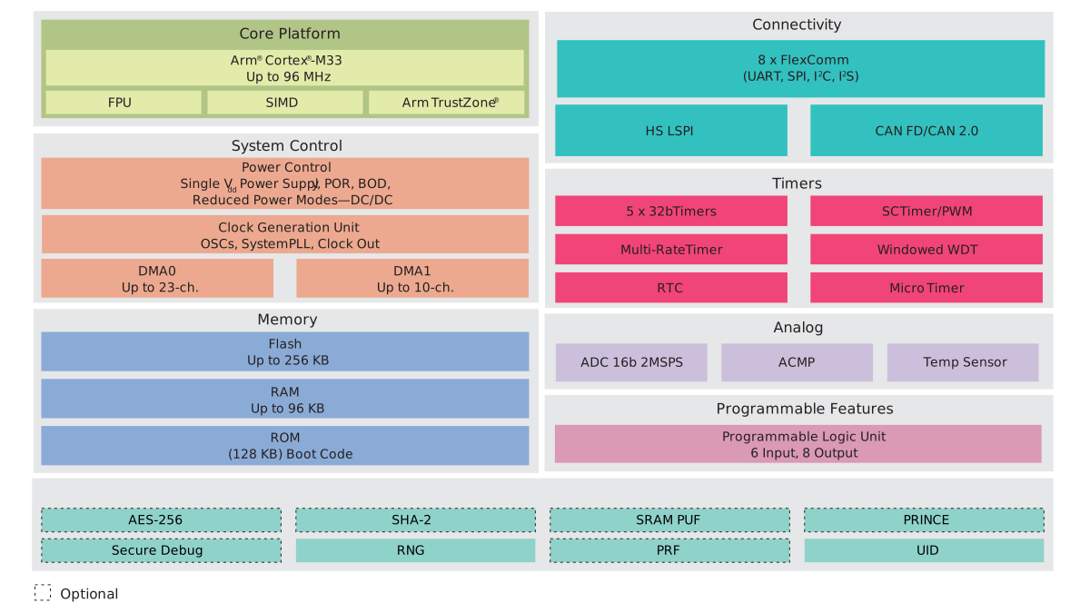
Block Diagram

LPC550x MCU

LPC550x MCU

Features

Arm Cortex-M33 Core

  • Running at frequency of up to 96 MHz
  • Arm TrustZone®, floating point unit (FPU) and memory protection unit (MPU)
  • Cortex-M33 built-in nested vectored interrupt controller (NVIC)
  • Non-maskable interrupt (NMI) input with a selection of sources
  • Serial wire debug with eight breakpoints and four watch points. Includes serial wire output for enhanced debug capabilities
  • System tick timer

On-Chip Memory

  • Up to 256 KB on-chip flash program memory with flash accelerator and 512 byte page erase and write
  • Up to 96 KB total SRAM consisting of 16 KB SRAM on code bus, 64 KB SRAM on system bus (64 KB is contiguous), and additional 16 KB SRAM on system bus

Security Features

  • Arm TrustZone® enabled
  • PRINCE module for real-time encryption of data being written to on-chip flash and decryption of encrypted flash data during read to allow asset protection*
  • CASPER crypto coprocessor is provided to enable hardware acceleration for various functions required for certain asymmetric cryptographic algorithms, such as elliptic curve cryptography (ECC)
  • AES-256 encryption/decryption engine*
  • Secure hash algorithm (SHA2) module supporting secure boot with dedicated DMA controller*
  • Physical unclonable function (PUF) using dedicated SRAM for silicon fingerprint. PUF can generate, store, and reconstruct key sizes from 64 bits to 4096 bits. Includes hardware for key extraction*
  • 128-bit unique device serial number for identification (UUID)*
  • Secure GPIO*
  • True random number generator (TRNG)
  • Code watchdog

Serial Interfaces

  • The FlexComm interface contains up to nine serial peripherals. Each FlexComm interface can be selected by software to be a USART, SPI, I²C and I²S interface
  • I²C-bus interfaces support Fast-mode and fast-mode plus with data rates of up to 1 Mbit/s and with multiple address recognition and monitor mode

Digital Peripherals

  • DMA0 controller with 22 channels and up to 22 programmable triggers, able to access all memories and DMA-capable peripherals
  • DMA1 controller with 10 channels and up to 15 programmable triggers, able to access all memories and DMA-capable peripherals
  • CAN FD module with dedicated DMA controller
  • CRC engine block can calculate a CRC on supplied data using one of three standard polynomials with DMA support
  • Up to 45 general-purpose input/output (GPIO) pins
  • GPIO registers are located on the AHB for fast access. The DMA supports GPIO ports
  • Up to eight GPIOs can be selected as pin interrupts (PINT), triggered by rising, falling or both input edges
  • Two GPIO grouped interrupts (GINT) enable an interrupt based on a logical (AND/OR) combination of input states
  • I/O pin configuration with support for up to 16 function options
  • Programmable logic unit (PLU) to create small combinational and/or sequential logic networks including state machines

Analog Peripherals

  • 16-bit ADC with five differential channel pair (or 10 single-ended channels), and with multiple internal and external trigger inputs and sample rates of up to 2.0 M samples/sec. In single-ended mode, the ADC supports 2 simultaneous conversions, on input channels belonging to a differential pair
  • Integrated temperature sensor connected to the ADC
  • Comparator with five input pins and external or internal reference voltage

Timers

  • Five 32-bit standard general purpose asynchronous timers/counters that support up to four capture inputs and four compare outputs. Specific timer events can be selected to generate DMA requests
  • One SCTimer/PWM with eight input and 10 output functions (including 16 capture and match registers). Inputs and outputs can be routed to/from external pins and internally to/from selected peripherals. Internally, the SCTimer/PWM supports 16 match/captures, 16 events and 32 states
  • 32-bit Real-time clock (RTC) with 1 s resolution running in the always-on power domain. Another timer in the RTC can be used for wake-up from all low-power modes including deep power down, with 1 ms resolution
  • Multiple-channel multi-rate 24-bit timer (MRT) for repetitive interrupt generation at up to four programmable, fixed rates
  • Windowed watchdog timer (WWDT) with FRO 1 MHZ as a clock source
  • Micro-tick timer running from the watchdog oscillator can be used to wake the device up from sleep and deep-sleep modes
  • 42-bit free running OS Timer as a continuous timebase for the system, available in any reduced power modes

Clock Generation

  • 96 MHz/12 MHz internal free running oscillator (FRO). This oscillator provides a selectable 96 MHz output, and a divided down 12 MHz output that can be used as a system clock. The FRO is trimmed to +/- 1% accuracy over the entire voltage (from 0 C to 85 C). The FRO is trimmed to +/- 2% accuracy over the entire voltage and -40 °C to 105 °C
  • 32.768 kHz internal free running oscillator (FRO) with +/- 2% accuracy over the entire voltage and -40 C to 105 C
  • 1 MHz internal low-power oscillator
  • Crystal oscillator with an operating frequency of 12 MHz to 32 MHz. Option for external clock input (bypass mode) for clock frequencies of up to 25 MHz
  • Crystal oscillator with 32.768 kHz operating frequency
  • PLL0 and PLL1 allows CPU operation up to the maximum CPU rate without the need for a high-frequency external clock
  • Clock output function with divider to monitor internal clocks
  • Frequency measurement unit for measuring the frequency of any on-chip or off-chip clock signal

Power-Saving Modes

  • Integrated Power Management Unit (PMU) to minimize power consumption
  • Reduced power modes: Sleep, deep sleep with RAM retention, power down with RAM and CPU retention, and deep power down with RAM retention
  • Configurable wake-up options from peripheral interrupts
  • The micro-tick timer running from the watchdog oscillator, and the real-time clock (RTC) running from the 32.678 kHz clock, can be used to wake the device up from sleep and deep-sleep modes
  • Power-on reset (POR)
  • Brown-out-detectors (BOD) with separate thresholds for interrupt and forced reset

Additional Information

  • Operating from an internal DC-DC converter
  • Single power supply 1.8 V to 3.6 V
  • JTAG boundary scan supported
  • Operating temperature range -40 °C to +105 °C
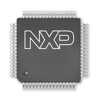
  • Available in HTQFP64 and HVQFN48 packages

Buy/Parametrics


Documentation

Quick reference to our documentation types

1-10 of 25 documents

Compact List

Application Note (16)
Application Note Software (4)
Data Sheet (2)
Errata (1)
Fact Sheet (1)
User Guide (1)

Design Resources

Design Files

Quick reference to our design files types.

3 design files

Hardware

Quick reference to our board types.

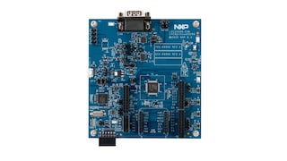
1-5 of 9 hardware offerings

Show All

Software

Quick reference to our software types.

1-5 of 13 software files

Show All

Note: For better experience, software downloads are recommended on desktop.

Training

22 trainings

Show All