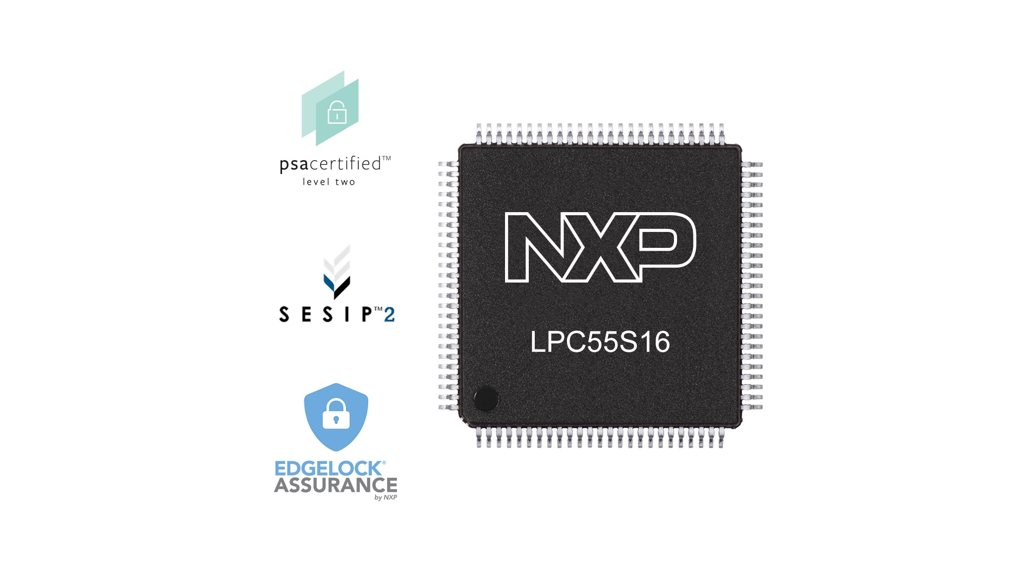


EdgeLock® Assurance
Proven security development processes and verification assessments – from product concept through release – help ensure customers receive trusted solutions for their security challenges.
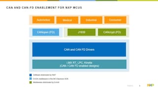
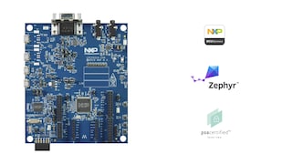
The LPC551x/S1x MCU family is part of the EdgeVerse™ edge computing platform and expands the world’s first general purpose Cortex-M33-based MCU series, offering significant advantages for developers, including pin-, software- and peripheral-compatibility for ease of use and to accelerate time to market, while leveraging the cost-effective 40-nm NVM process technology.
The LPC551x/S1x is the baseline family within the LPC5500 MCU series inclusive of LPC5516x, LPC55S16x, LPC5514x, LPC55S14x, LPC5512x MCUs, providing new levels of cost and performance efficiency in addition to advanced security and system integration for industrial and general embedded markets.
Built with advanced security in mind, the LPC55S16 MCU is part of the Certified EdgeLock® Assurance program and has been awarded Level 2 certifications by both the PSA Certified™ scheme co-developed by Arm and the GlobalPlatform Security Evaluation Standard for IoT Platforms (SESIP).
Proven security development processes and verification assessments – from product concept through release – help ensure customers receive trusted solutions for their security challenges.
LPC810 and LPC830: 32-Bit Arm® Cortex®-M0+-Based Low-Cost MCU

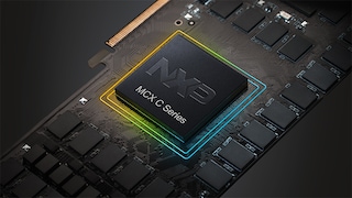
MCX C04x MCUs with Arm® Cortex® M0+, Entry Level MCUs with Classical Peripherals
MCX A13, 14, 15 Essential MCUs with Arm® Cortex® M33, Low Power and Intelligent Peripherals
LPC820: 32-Bit Arm® Cortex®M0+-Based Low-Cost MCU
MCX C14x/24x/44x MCUs with Arm® Cortex® M0+, Entry level MCUs with USB, Segment LCD and Classical Peripherals

LPC860: 32-Bit Arm® Cortex®-M0+-Based Low-Cost MCU with I3C Interface
|
|
|
|
|
|
|
|---|---|---|---|---|---|
|
|
|
|
|
|
|
|
|
|
|
|
|
|
|
|
|
|
|
|
|
|
|
|
|
|
|
|
|
|
|
|
|
|
|
|
|
|
|
|
|
|
|
|
|
|
|
|
|
|
|
|
|
|
|
|
|
|
|
|
|
|
|
|
|
|
|
|
|
|
Quick reference to our documentation types
1-10 of 40 documents
Compact List
1-5of 19 design files
Receive the full breakdown. See the product footprint and more in the eCad file.
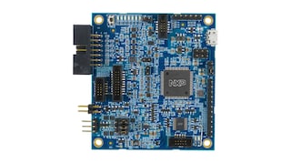
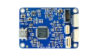
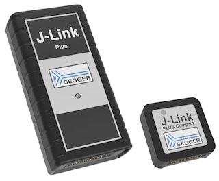
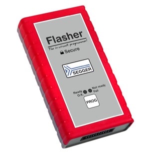
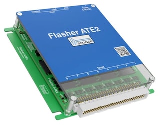
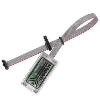
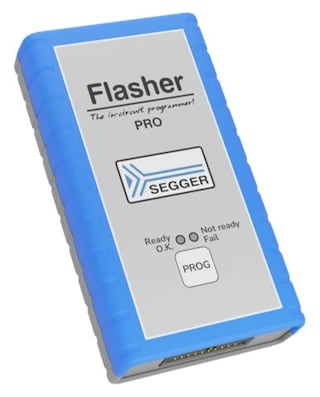
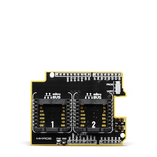
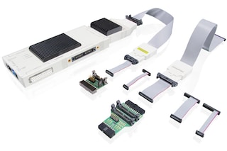
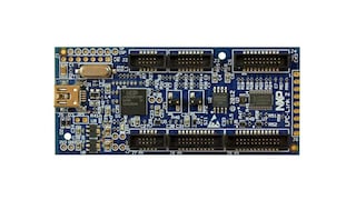
1-5 of 9 hardware offerings
Additional hardware available. View our featured partner solutions.
Quick reference to our software types.
1-5 of 16 software files
Additional software available. View our featured partner solutions.
Note: For better experience, software downloads are recommended on desktop.
To get further assistance directly from NXP, please see our Engineering Services.
1-5 of 10 engineering services


To find additional partner offerings that support this product, visit our Partner Marketplace.