
Safety System Basis Chip with Low Power, for ASIL D Systems
The LPC552x/S2x MCU family is part of the EdgeVerse™ edge computing platform and further expands the world’s first general purpose Cortex-M33-based MCU series, offering significant advantages for developers, including pin-, software- and peripheral-compatibility for ease of use and accelerating time to market, while leveraging the cost-effective 40-nm NVM process technology.
The LPC552x/S2x is a mainstream family within the LPC5500 MCU series inclusive of LPC55S28, LPC55S26, LPC5528, LPC5526 MCUs, providing a perfect balance between security, performance efficiency and system integration for general embedded and industrial IoT markets. The LPC552x/S2x MCU family combines the high-performance efficiency of the Cortex-M33 core with multiple high-speed interfaces, an integrated power management IC, and rich analog integration.
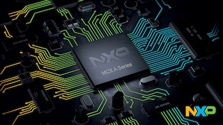
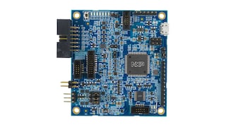
MCX A13, 14, 15 Essential MCUs with Arm® Cortex® M33, Low Power and Intelligent Peripherals
High Efficiency Arm® Cortex®-M33-Based Microcontroller Family
|
|
|
|
|
|
|
|---|---|---|---|---|---|
|
|
|
|
|
|
|
|
|
|
|
|
|
|
|
|
|
|
|
|
|
|
|
|
|
|
|
|
|
|
|
|
|
|
|
|
|
|
|
|
|
|
|
|
|
|
|
|
|
|
|
|
|
|
|
|
|
|
|
|
|
|
|
|
|
|
|
|
|
|
Quick reference to our documentation types
1-10 of 54 documents
Compact List
1-5of 16 design files
Receive the full breakdown. See the product footprint and more in the eCad file.
1-5 of 9 hardware offerings
Quick reference to our software types.
1-5 of 18 software files
Additional software available. View our featured partner solutions.
Note: For better experience, software downloads are recommended on desktop.
To get further assistance directly from NXP, please see our Engineering Services.
1-5 of 11 engineering services


To find additional partner offerings that support this product, visit our Partner Marketplace.