


Safety System Basis Chip with Low Power, for ASIL D Systems
The LPC553x/S3x MCU family further expands the general purpose Cortex-M33-based MCU series, offering significant performance enhancement, all on-chip RAM with Parity or ECC, renewed security features and precision analog additions, leveraging the cost-effective 40-nm NVM process technology.
The LPC553x/S3x family includes a proprietary DSP accelerator offering 10x clock cycle reduction, bringing significant signal processing efficiency gains.
MCX N94, N54, N53, N52 and N24 with Highly Integrated Low-power Dual Core Arm® Cortex®-M33 MCUs, with on-chip Accelerators and Advanced Security
MCX A13, 14, 15 Essential MCUs with Arm® Cortex® M33, Low Power and Intelligent Peripherals
MCX N23x Highly Integrated MCUs with On-Chip Accelerators, Intelligent Peripherals and Advanced Security
|
|
|
|
|
|
|
|---|---|---|---|---|---|
|
|
|
|
|
|
|
|
|
|
|
|
|
|
|
|
|
|
|
|
|
|
|
|
|
|
|
|
|
|
|
|
|
|
|
|
|
|
|
|
|
|
|
|
|
|
|
|
|
|
|
|
|
|
|
|
|
|
|
|
|
|
|
|
|
|
|
|
|
|
Quick reference to our documentation types
1-10 of 67 documents
Compact List
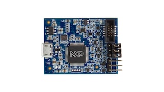
1-5of 11 design files
Receive the full breakdown. See the product footprint and more in the eCad file.
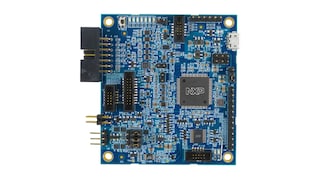
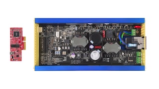
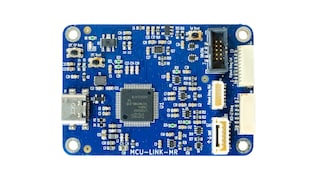
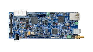
1-5 of 12 hardware offerings
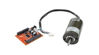
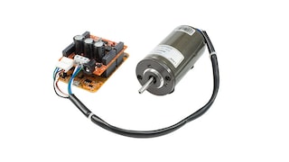
Additional hardware available. View our featured partner solutions.
Quick reference to our software types.
1-5 of 14 software files
Additional software available. View our featured partner solutions.
Note: For better experience, software downloads are recommended on desktop.
To get further assistance directly from NXP, please see our Engineering Services.
1-5 of 7 engineering services

To find additional partner offerings that support this product, visit our Partner Marketplace.