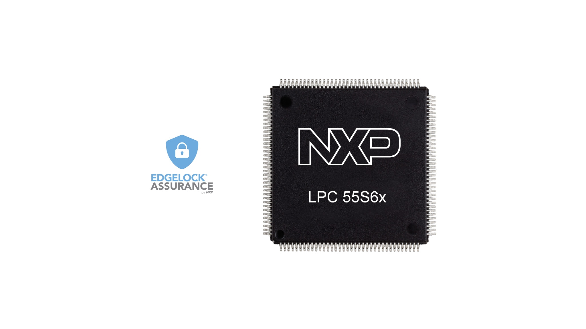
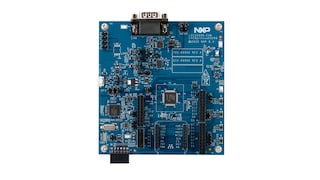
LPC550x/S0x: Baseline Arm® Cortex®-M33-Based Microcontroller Family

Roll over image to zoom in

Block Diagram

LPC550x MCU

LPC550x MCU

Features

Arm Cortex-M33 Core

  • Running at frequency of up to 96 MHz
  • Arm TrustZone®, floating point unit (FPU) and memory protection unit (MPU)
  • Cortex-M33 built-in nested vectored interrupt controller (NVIC)
  • Non-maskable interrupt (NMI) input with a selection of sources
  • Serial wire debug with eight breakpoints and four watch points. Includes serial wire output for enhanced debug capabilities
  • System tick timer

On-Chip Memory

  • Up to 256 KB on-chip flash program memory with flash accelerator and 512 byte page erase and write
  • Up to 96 KB total SRAM consisting of 16 KB SRAM on code bus, 64 KB SRAM on system bus (64 KB is contiguous), and additional 16 KB SRAM on system bus

Security Features

  • Arm TrustZone® enabled
  • PRINCE module for real-time encryption of data being written to on-chip flash and decryption of encrypted flash data during read to allow asset protection*
  • CASPER crypto coprocessor is provided to enable hardware acceleration for various functions required for certain asymmetric cryptographic algorithms, such as elliptic curve cryptography (ECC)
  • AES-256 encryption/decryption engine*
  • Secure hash algorithm (SHA2) module supporting secure boot with dedicated DMA controller*
  • Physical unclonable function (PUF) using dedicated SRAM for silicon fingerprint. PUF can generate, store, and reconstruct key sizes from 64 bits to 4096 bits. Includes hardware for key extraction*
  • 128-bit unique device serial number for identification (UUID)*
  • Secure GPIO*
  • True random number generator (TRNG)
  • Code watchdog

Serial Interfaces

  • The FlexComm interface contains up to nine serial peripherals. Each FlexComm interface can be selected by software to be a USART, SPI, I²C and I²S interface
  • I²C-bus interfaces support Fast-mode and fast-mode plus with data rates of up to 1 Mbit/s and with multiple address recognition and monitor mode

Digital Peripherals

  • DMA0 controller with 22 channels and up to 22 programmable triggers, able to access all memories and DMA-capable peripherals
  • DMA1 controller with 10 channels and up to 15 programmable triggers, able to access all memories and DMA-capable peripherals
  • CAN FD module with dedicated DMA controller
  • CRC engine block can calculate a CRC on supplied data using one of three standard polynomials with DMA support
  • Up to 45 general-purpose input/output (GPIO) pins
  • GPIO registers are located on the AHB for fast access. The DMA supports GPIO ports
  • Up to eight GPIOs can be selected as pin interrupts (PINT), triggered by rising, falling or both input edges
  • Two GPIO grouped interrupts (GINT) enable an interrupt based on a logical (AND/OR) combination of input states
  • I/O pin configuration with support for up to 16 function options
  • Programmable logic unit (PLU) to create small combinational and/or sequential logic networks including state machines

Analog Peripherals

  • 16-bit ADC with five differential channel pair (or 10 single-ended channels), and with multiple internal and external trigger inputs and sample rates of up to 2.0 M samples/sec. In single-ended mode, the ADC supports 2 simultaneous conversions, on input channels belonging to a differential pair
  • Integrated temperature sensor connected to the ADC
  • Comparator with five input pins and external or internal reference voltage

Timers

  • Five 32-bit standard general purpose asynchronous timers/counters that support up to four capture inputs and four compare outputs. Specific timer events can be selected to generate DMA requests
  • One SCTimer/PWM with eight input and 10 output functions (including 16 capture and match registers). Inputs and outputs can be routed to/from external pins and internally to/from selected peripherals. Internally, the SCTimer/PWM supports 16 match/captures, 16 events and 32 states
  • 32-bit Real-time clock (RTC) with 1 s resolution running in the always-on power domain. Another timer in the RTC can be used for wake-up from all low-power modes including deep power down, with 1 ms resolution
  • Multiple-channel multi-rate 24-bit timer (MRT) for repetitive interrupt generation at up to four programmable, fixed rates
  • Windowed watchdog timer (WWDT) with FRO 1 MHZ as a clock source
  • Micro-tick timer running from the watchdog oscillator can be used to wake the device up from sleep and deep-sleep modes
  • 42-bit free running OS Timer as a continuous timebase for the system, available in any reduced power modes

Clock Generation

  • 96 MHz/12 MHz internal free running oscillator (FRO). This oscillator provides a selectable 96 MHz output, and a divided down 12 MHz output that can be used as a system clock. The FRO is trimmed to +/- 1% accuracy over the entire voltage (from 0 C to 85 C). The FRO is trimmed to +/- 2% accuracy over the entire voltage and -40 °C to 105 °C
  • 32.768 kHz internal free running oscillator (FRO) with +/- 2% accuracy over the entire voltage and -40 C to 105 C
  • 1 MHz internal low-power oscillator
  • Crystal oscillator with an operating frequency of 12 MHz to 32 MHz. Option for external clock input (bypass mode) for clock frequencies of up to 25 MHz
  • Crystal oscillator with 32.768 kHz operating frequency
  • PLL0 and PLL1 allows CPU operation up to the maximum CPU rate without the need for a high-frequency external clock
  • Clock output function with divider to monitor internal clocks
  • Frequency measurement unit for measuring the frequency of any on-chip or off-chip clock signal

Power-Saving Modes

  • Integrated Power Management Unit (PMU) to minimize power consumption
  • Reduced power modes: Sleep, deep sleep with RAM retention, power down with RAM and CPU retention, and deep power down with RAM retention
  • Configurable wake-up options from peripheral interrupts
  • The micro-tick timer running from the watchdog oscillator, and the real-time clock (RTC) running from the 32.678 kHz clock, can be used to wake the device up from sleep and deep-sleep modes
  • Power-on reset (POR)
  • Brown-out-detectors (BOD) with separate thresholds for interrupt and forced reset

Additional Information

  • Operating from an internal DC-DC converter
  • Single power supply 1.8 V to 3.6 V
  • JTAG boundary scan supported
  • Operating temperature range -40 °C to +105 °C
  • Available in HTQFP64 and HVQFN48 packages

Part numbers include: LPC5502JBD64, LPC5502JHI48, LPC5504JBD64, LPC5504JHI48, LPC5506JBD64, LPC5506JHI48, LPC55S04JBD64, LPC55S04JHI48, LPC55S06JBD64, LPC55S06JHI48.

Buy/Parametrics


Documentation

Quick reference to our documentation types.

1-5 of 25 documents

Show All

Design Files

Quick reference to our design files types.

3 design files

Hardware

Quick reference to our board types.

1-5 of 7 hardware offerings
Show All

Software

Quick reference to our software types.

1-5 of 12 software files

Show All

Note: For better experience, software downloads are recommended on desktop.

Engineering Services

1-5 of 8 engineering services

Show All

To find additional partner offerings that support this product, visit our Partner Marketplace.

Training

21 trainings

Show All