
Kinetis KV4x-168 MHz, High Performance Motor / Power Conversion MCUs based on Arm® Cortex®-M4
The MCX A26 family of microcontrollers delivers robust performance with clock speeds up to 240 MHz, featuring up to 1MB of Flash and 256kB of RAM. Engineered for PC accessory applications, these devices offer a comprehensive set of serial peripherals including full-speed USB, dual CAN-FD, I3C and support for 4 x 44-segment LCD displays. FlexIO and SmartDMA enhance flexibility and data handling, while integrated security features ensure reliable operation.
The MCX A265 and A266 are also optimized for motor control, incorporating two FlexPWM modules with four submodules each, AOI logic, and up to two ADCs for precise signal processing.
Development is supported by the MCUXpresso Developer Experience, designed to simplify workflows and accelerate embedded system design.

MCX A18: Essential Mainstream Arm® Cortex® M33 MCU with 240MHz and Motor Control Peripherals
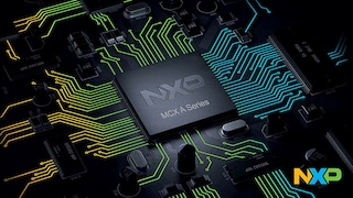
MCX A13, 14, 15 Essential MCUs with Arm® Cortex® M33, Low Power and Intelligent Peripherals
High Efficiency Arm® Cortex®-M33-Based Microcontroller Family
MCX N94, N54, N53, N52 and N24 with Highly Integrated Low-power Dual Core Arm® Cortex®-M33 MCUs, with on-chip Accelerators and Advanced Security
LPC552x/S2x: Mainstream Arm® Cortex®-M33-based Microcontroller Family
|
|
|
|
|
|
|
|---|---|---|---|---|---|
|
|
|
|
|
|
|
|
|
|
|
|
|
|
|
|
|
|
|
|
|
|
|
|
|
|
|
|
|
|
|
|
|
|
|
|
|
|
|
|
|
|
|
|
|
|
|
|
|
|
|
|
|
|
|
|
|
|
|
|
|
|
|
|
|
|
|
|
|
|
Quick reference to our documentation types
1-10 of 12 documents
Compact List
Please wait while your secure files are loading.
2 design files
Receive the full breakdown. See the product footprint and more in the eCad file.
Please wait while your secure files are loading.
3 hardware offerings
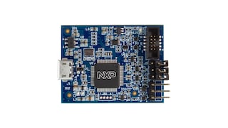
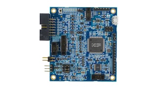
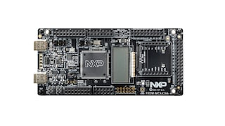
1-5 of 16 hardware offerings
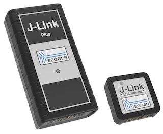
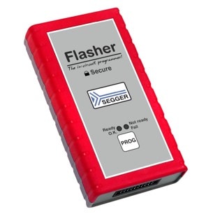
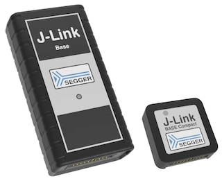
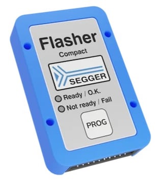
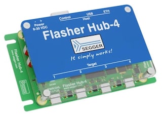
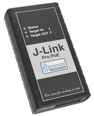
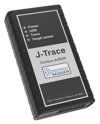
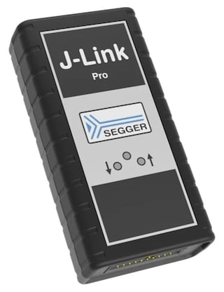
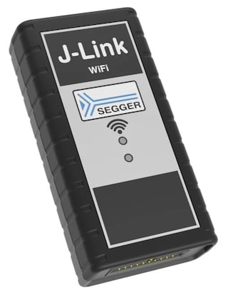
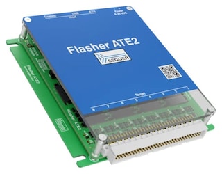
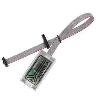
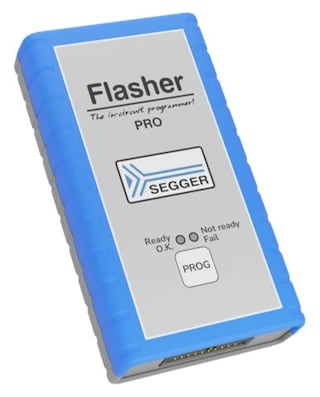
To find additional partner offerings that support this product, visit our Partner Marketplace.
Quick reference to our software types.
5 software files
Additional software available. View our featured partner solutions.
Note: For better experience, software downloads are recommended on desktop.
Please wait while your secure files are loading.
1-5 of 19 software offerings


To find additional partner offerings that support this product, visit our Partner Marketplace.