Data Sheet (1)
Package Information (1)
Packing Information (2)
User Guide (1)
-
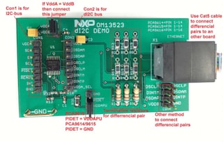
User manual for dI2C demo board[UM10856]
The PCA9615 is a Fast-mode Plus (Fm+) SMBus/I²C-bus buffer that extends the normal single-ended SMBus/I²C-bus through electrically noisy environments using a differential SMBus/I²C-bus (dI²C) physical layer, which is transparent to the SMBus/I²C-bus protocol layer. It consists of two single-ended to differential driver channels for the SCL (serial clock) and SDA (serial data).
The use of differential transmission lines between identical dI²C bus buffers removes electrical noise and common-mode offsets that are present when signal lines must pass between different voltage domains, are bundled with hostile signals, or run adjacent to electrical noise sources, such as high energy power supplies and electric motors.
The SMBus/I²C-bus was conceived as a simple slow speed digital link for short runs, typically on a single PCB or between adjacent PCBs with a common ground connection. Applications that extend the bus length or run long cables require careful design to preserve noise margin and reject interference.
The dI²C-bus buffers were designed to solve these problems and are ideally suited for rugged high noise environments and/or longer cable applications, allow multiple followers, and operate at bus speeds up to 1 MHz clock rate. Cables can be extended to at least 3 meters (3 m), or longer cable runs at lower clock speeds. The dI²C-bus buffers are compatible with existing SMBus/I²C-bus devices and can drive Standard, Fast-mode, and Fast-mode Plus devices on the single-ended side.
Signal direction is automatic, and requires no external control. To prevent bus latch up, the standard SMBus/I²C-bus side of the bus buffer, the PCA9615 employs static offset, care should be taken when connecting these to other SMBus/I²C-bus buffers that may not operate with offset.
This device is a bridge between the normal 2-wire single-ended wired-OR SMBus/I²C-bus and the 4-wire dI²C-bus.
Additional circuitry allows the PCA9615 to be used for ‘hot swap’ applications, where systems are always on, but require insertion or removal of modules or cards without disruption to existing signals.
The PCA9615 has two supply voltages, VDD(A) and VDD(B). VDD(A), the card side supply, only serves as a reference and ranges from 2.3 V to 5.5 V. VDD(B), the line side supply, serves as the majority supply for circuitry and ranges from 3.0 V to 5.5 V.
|
|
|
|
|
|
|
|---|---|---|---|---|---|
|
|
|
|
|
|
|
|
|
|
|
|
|
|
|
|
|
|
|
|
|
|
|
|
|
|
|
|
|
|
|
|
|
|
|
|
|
|
|
|
|
|
|
|
|
|
|
|
|
|
|
|
|
|
|
|
|
|
|
|
|
|
|
|
|
|
|
|
|
|
Quick reference to our documentation types
5 documents
Compact List
1 design file
Receive the full breakdown. See the product footprint and more in the eCad file.
To get further assistance directly from NXP, please see our Engineering Services.
2 engineering services

To find additional partner offerings that support this product, visit our Partner Marketplace.