


Product Longevity
Participating products are available for a minimum of 10 years. Designated participating products developed for the automotive, telecom and medical segments are available for a minimum of 15 years.
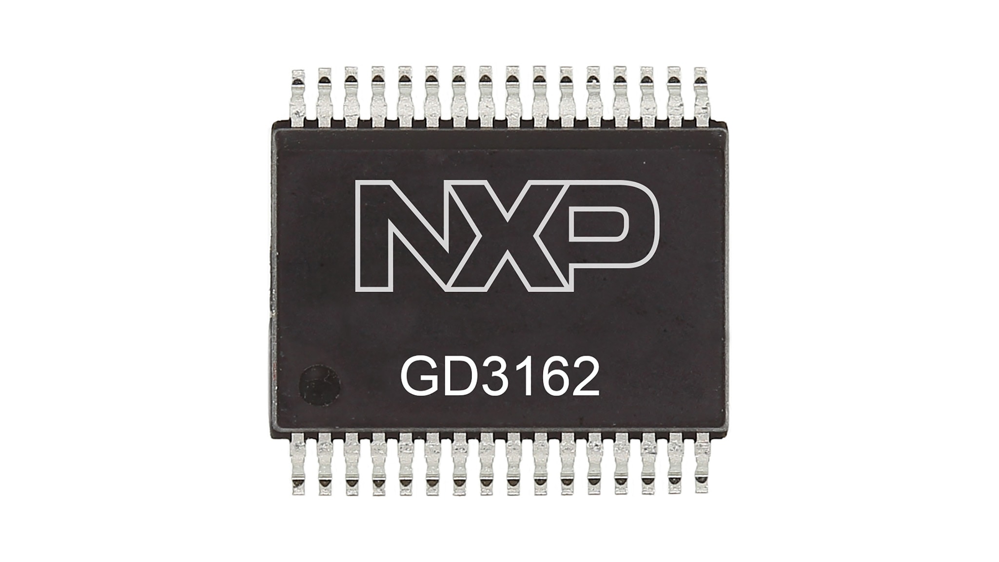
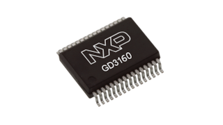
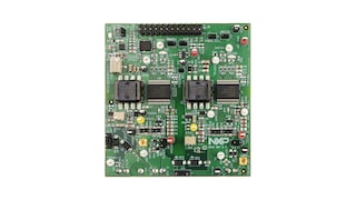
The GD3162 is an advanced, galvanically-isolated, single-channel gate driver designed to drive the latest SiC and IGBT modules for xEV traction inverters.
The GD3162 offers an adjustable dynamic gate strength drive via a programmable interface over SPI. In addition, advanced programmable protection features are autonomously managed as faults and the status of the power device and gate driver are reported via the interrupt pins.
The GD3162 is designed for high-functional safety integrity level systems (ASIL C/D) and meets the stringent requirements of automotive applications, being fully AEC-Q100 grade 1 qualified.
Participating products are available for a minimum of 10 years. Designated participating products developed for the automotive, telecom and medical segments are available for a minimum of 15 years.
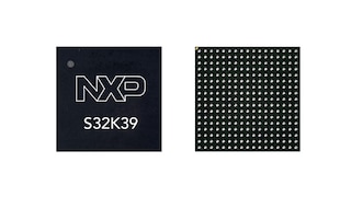
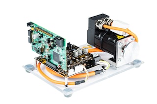
S32K39/37/36 Microcontrollers for Electrification Applications
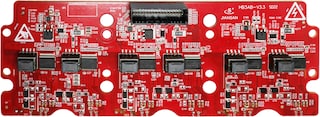
Advanced High Voltage Isolated Gate Driver with Segmented Drive for SiC MOSFETs
|
|
|
|
|
|
|
|---|---|---|---|---|---|
|
|
|
|
|
|
|
|
|
|
|
|
|
|
|
|
|
|
|
|
|
|
|
|
|
|
|
|
|
|
|
|
|
|
|
|
|
|
|
|
|
|
|
|
|
|
|
|
|
|
|
|
|
|
|
|
|
|
|
|
|
|
|
|
|
|
|
|
|
|
Quick reference to our documentation types
6 documents
Compact List
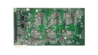
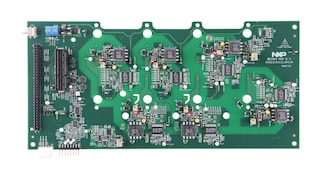
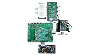
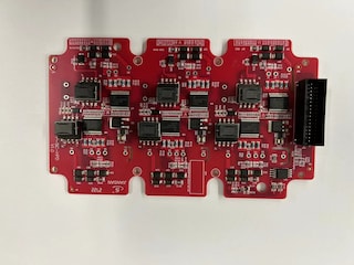
1-5 of 8 hardware offerings
Additional hardware available. View our featured partner solutions.
Quick reference to our software types.
3 software files
Note: For better experience, software downloads are recommended on desktop.