デザイン・ファイル
1 設計・ファイル
-
プリント基板と回路図
OrCAD symbols for MPC8349E TBGA device
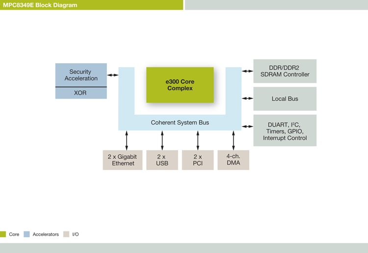
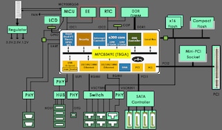
The MPC8349E PowerQUICC® II Pro family of integrated communications processors is a next-generation extension of the popular PowerQUICC II line. Based on system-on-chip (SoC) architecture, the MPC8349E PowerQUICC II Pro family integrates the enhanced e300 core and advanced features such as double data rate (DDR) memory, dual Gigabit Ethernet (GbE), dual PCI and high-speed USB controllers. With clock speeds scaling to 667 MHz, the MPC8349E family of processors offers the highest performing PowerQUICC II devices available.
The MPC8349E PowerQUICC II Pro family is designed to provide a cost-effective, highly integrated control processing solution that addresses the emerging needs of networking, communications and pervasive computing applications. MPC8349E processors can be used in applications such as Ethernet routers and switches, wireless LAN (WLAN) equipment, network storage, home network appliances, industrial control equipment, and copiers, printers and other imaging systems.
部品番号: MPC8349CVVAJDB, MPC8349CZUAJDB, MPC8349ECVVAGDB, MPC8349ECVVAJDB, MPC8349ECVVAJFB, MPC8349ECZUAJDB, MPC8349EVVAGDB, MPC8349EVVAJDB, MPC8349EVVAJFB, MPC8349EVVALFB, MPC8349EZUALFB, MPC8349VVAGDB, MPC8349VVAJDB, MPC8349VVAJFB, MPC8349VVALFB.
クイック・リファレンス ドキュメンテーションの種類.
1-5 の 59 ドキュメント
1 設計・ファイル
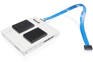
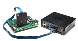
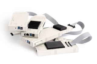
4 ハードウェア提供
追加ハードウェアを利用可能 パートナー・ソリューションの特集を表示.
1-5 の 6 ソフトウェア・ファイル
追加ソフトウェアを利用可能 パートナー・ソリューションの特集を表示.
注: より快適にご利用いただくために、ソフトウェアのダウンロードはデスクトップで行うことを推奨します。
NXPから直接サポートを受けるには、以下のサイトをご覧ください。 エンジニアリング・サービス.
1-5 の 13 エンジニアリング・サービス


本製品をサポートするパートナーの一覧は、 パートナーマーケットプレイス.
1-5 of 15 トレーニング


.svg?imwidth=300)
