
Kinetis® K24-120 MHz, Full-Speed USB, 256KB SRAM Microcontrollers (MCUs) based on Arm® Cortex®-M4 Core
The Kinetis K28 USB Arm® Cortex®-M4 MCUs target applications requiring processing efficiency and extra-large embedded memory with 2 MB Flash and 1 MB SRAM. This microcontroller sub-family is:
3 Input supply voltage rails: (1.2V, 1.8V and 3V) + separate VBAT domain
K28 implements a Power Management Controller supporting Core Voltage Bypass and can be powered by an external PMIC to maximize the power efficiency of the overall system
Packages: 169 MAPBGA (9x9mm2, 0.65mm pitch) and 210 WLCSP (6.9x6.9mm2, 0.4 mm pitch)
Evaluation / Development platform: FRDM-K28F
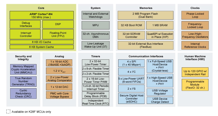
Note: To see the product features close this window.
Part numbers include: KK28FN2M0CAU15, MK28FN2M0ACAU15, MK28FN2M0AVMI15, MK28FN2M0CAU15, MK28FN2M0VMI15.
| Kinetis MCU sub-family | Part # | Mask Set | Flash | SRAM | PMC w/ Core Voltage Bypass | Packages | Development board |
|---|---|---|---|---|---|---|---|
| K28 | MK28FN2M0ACAU15R | 3N96T (recommended) |
2 MB | 1 MB | Yes | 210 WLCSP | FRDM-K28F |
| MK28FN2M0AVMI15 | 169 MAPBGA | ||||||
| MK28FN2M0CAU15R | 2N96T | 210 WLCSP | |||||
| MK28FN2M0VMI15 | 169 MAPBGA | ||||||
| K27 | MK27FN2M0AVMI15 | 3N96T (recommended) |
No | 169 MABPGA | |||
| MK27FN2M0VMI15 | 2N96T |
Quick reference to our documentation types.
1-5 of 60 documents
Please wait while your secure files are loading.
2 design files
Please wait while your secure files are loading.
1-5 of 9 hardware offerings
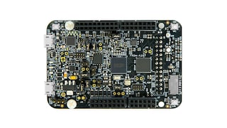
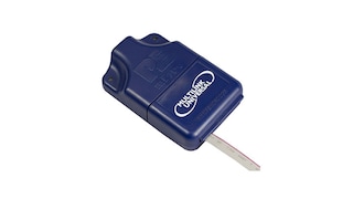
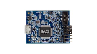
Additional hardware available. View our featured partner solutions.
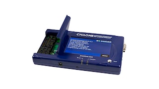
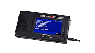
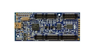
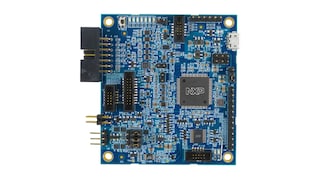
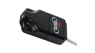

1 hardware offering
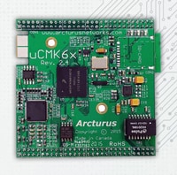
To find additional partner offerings that support this product, visit our Partner Marketplace.
Quick reference to our software types.
1-5 of 9 software files
Additional software available. View our featured partner solutions.
Note: For better experience, software downloads are recommended on desktop.
Please wait while your secure files are loading.
1-5 of 45 software offerings


.svg?imwidth=300)


.svg?imwidth=300)


To find additional partner offerings that support this product, visit our Partner Marketplace.
1-5 of 15 engineering services


.svg)


There are no results for this selection.
To find additional partner offerings that support this product, visit our Partner Marketplace.
5 trainings
Additional trainings are available. View our featured partner trainings.
5 trainings
To find additional partner offerings that support this product, visit our Partner Marketplace.