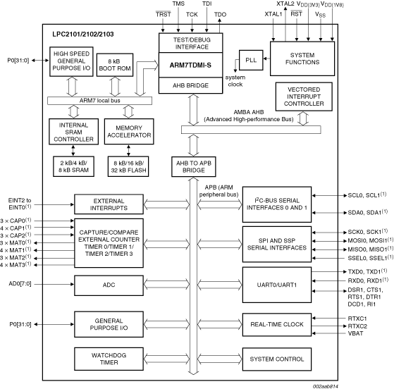
Single-chip 16-bit/32-bit microcontrollers; 8 kB/16 kB/32 kB flash with ISP/IAP, fast ports and 10-bit ADC

LPC2103FBD48
  • Not Recommended for New Designs
  • This page contains information on a product that is not recommended for new designs.

See product image

Product Details

Select a section:

Block Diagram

Block diagram: LPC2101FBD48, LPC2102FBD48, LPC2102FHN48, LPC2103FBD48, LPC2103FHN48

Features

Enhanced features

Enhanced features are available in parts LPC2101/02/03 labelled Revision A and higher:

  • Deep power-down mode with option to retain SRAM memory and/or RTC.
  • Three levels of flash Code Read Protection (CRP) implemented.

Key features

  • 16-bit/32-bit Arm7TDMI-S microcontroller in tiny LQFP48 and HVQFN48 packages.
  • 2 kB/4 kB/8 kB of on-chip static RAM and 8 kB/16 kB/32 kB of on-chip flash program memory. 128-bit wide interface/accelerator enables high-speed 70 MHz operation.
  • ISP/IAP via on-chip bootloader software. Single flash sector or full chip erase in 100 ms and programming of 256 bytes in 1 ms.
  • EmbeddedICE-RT offers real-time debugging with the on-chip RealMonitor software.
  • The 10-bit ADC provides eight analog inputs, with conversion times as low as 2.44 us per channel and dedicated result registers to minimize interrupt overhead.
  • Two 32-bit timers/external event counters with combined seven capture and seven compare channels.
  • Two 16-bit timers/external event counters with combined three capture and seven compare channels.
  • Low power Real-Time Clock (RTC) with independent power and dedicated 32 kHz clock input.
  • Multiple serial interfaces including two UARTs (16C550), two Fast I²C-buses (400 kbit/s), SPI and SSP with buffering and variable data length capabilities.
  • Vectored interrupt controller with configurable priorities and vector addresses.
  • Up to thirty-two, 5 V tolerant fast general purpose I/O pins.
  • Up to 13 edge or level sensitive external interrupt pins available.
  • 70 MHz maximum CPU clock available from programmable on-chip PLL with a possible input frequency of 10 MHz to 25 MHz and a settling time of 100 us.
  • On-chip integrated oscillator operates with an external crystal in the range from 1 MHz to 25 MHz.
  • Power saving modes include Idle mode, Power-down mode with RTC active, and Power-down mode.
  • Individual enable/disable of peripheral functions as well as peripheral clock scaling for additional power optimization.
  • Processor wake-up from Power-down and Deep power-down (Revision A and higher) mode via external interrupt or RTC.

Part numbers include: LPC2103FBD48.

Documentation

Quick reference to our documentation types.

1-5 of 27 documents

Show All

Design Resources

Select a section:

Design Files

1 design file

Support

What do you need help with?