Application Note (1)
Data Sheet (1)
-
A3G20S350-01S 2110-2170 MHz, 59 W Avg, 48 V GaN Data Sheet[A3G20S350-01S]
Package Information (1)
-
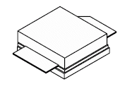
98ASA01061D[sot1828-3]
This A3G20S350-01S 59 W RF power GaN transistor is designed for cellular base station applications covering the frequency range of 2110 to 2170 MHz.
This part is characterized and performance is guaranteed for applications operating in the 2110 to 2170 MHz band. There is no guarantee of performance when this part is used in applications designed outside of these frequencies.
Typical Single-Carrier W-CDMA Performance: VDD = 48 Vdc, IDQ = 500 mA, Pout = 59 W Avg., Input Signal PAR = 9.9 dB @ 0.01% Probability on CCDF.
| Frequency | Gps (dB) |
ηD (%) |
Output PAR (dB) |
ACPR (dBc) |
| 2110 MHz | 18.0 | 37.0 | 7.0 | –33.3 |
| 2140 MHz | 18.0 | 36.9 | 7.0 | –33.3 |
| 2170 MHz | 18.1 | 37.0 | 6.9 | –32.3 |
|
|
|
|
|
|
|
|---|---|---|---|---|---|
|
|
|
|
|
|
|
|
|
|
|
|
|
|
|
|
|
|
|
|
|
|
|
|
|
|
|
|
|
|
|
|
|
|
|
|
|
|
|
|
|
|
|
|
|
|
|
|
|
|
|
|
|
|
|
|
|
|
|
|
|
|
|
|
|
|
|
|
|
|
Quick reference to our documentation types
3 documents
Compact List
2 design files
Receive the full breakdown. See the product footprint and more in the eCad file.